Fractilia adds overlay metrology capability
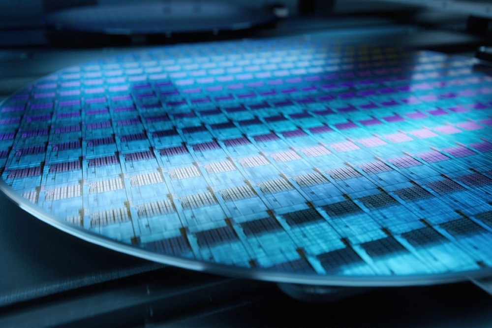
Fractilia Overlay Package offered as an optional feature for Fractilia’s MetroLER and FAME products, which have been adopted by dozens of industry-leading companies.
Fractilia has introduced the Fractilia Overlay Package, an optional offering that adds critical new overlay measurement and analysis capabilities to Fractilia’s MetroLER and FAME products. Fractilia’s products, which combine the company’s patented Fractilia Inverse Linescan Model (FILM) technology with true computational metrology, are the only proven fab solutions that provide highly accurate and precise measurements of all major stochastic effects – the single largest source of patterning errors at advanced nodes. Fractilia is currently engaged with multiple leading chip manufacturers in analyzing their SEM-based overlay data with the new Fractilia Overlay Package.
In semiconductor manufacturing, overlay is the precise placement of each patterned layer relative to a previous layer to ensure electrical contact and produce a functioning device. Optical-based metrology tools have traditionally been used by chip manufacturers to measure and control this pattern overlay, which is essential to producing high-yielding and high-performing semiconductor devices. These measurements are made on special targets in the scribe line rather than in the device itself. As feature sizes of chips continue to shrink and as stochastic variability has increased with the adoption of EUV patterning, there is a growing offset between what is measured in the scribe line and what is happening in the device. As a result, interest is growing in the use of SEM tools to measure overlay due to their higher resolution and precision compared to optical tools. However, SEMs introduce noise in the SEM image, which can be easily confused with stochastic variability on the wafer.
“SEM-based overlay measurements are increasingly being used to improve advanced patterning process control, but they are influenced by the same random and systematic SEM errors that affect other stochastics measurements,” stated Fractilia CTO Chris Mack. “Fractilia is unparalleled in measuring and subtracting out SEM noise through our proven FILM technology, and as a result, our customers are turning to Fractilia to help them apply our technology to improve the accuracy of their SEM overlay measurements. In addition, by combining SEM stochastics measurements with optical overlay measurements through our Fractilia Overlay Package, we believe that we not only can improve SEM overlay metrology accuracy, but also provide better lot dispositioning and correctables, which in turn can improve patterning control and reduce non-zero offset (NZO) or its variability.”
“Unbiased” Measurements Provide More Accurate Description of What’s on the Wafer
Fractilia’s FAME portfolio of solutions uses a proprietary and unique physics-based SEM modeling and data analysis approach that measures and subtracts the random and systematic errors from SEM images to provide measurements of what is on the wafer rather than what is on the images. FAME measures all major stochastic effects simultaneously, including line-edge roughness (LER) / linewidth roughness (LWR), local CD uniformity (LCDU), local edge placement error (LEPE), and stochastic defects, as well as provides CD measurements. It provides the highest signal-to-noise edge detection in the industry (up to 5x higher signal-to-noise ratio than other solutions), and extracts more than 30x more data from each SEM image.
With the new Fractilia Overlay Package, Fractilia adds highly accurate SEM-based overlay measurements, including their stochastic properties, on top of its existing measurement capabilities. Fractilia’s products have been adopted throughout the industry by dozens of companies, including leading semiconductor manufacturers, equipment companies, materials suppliers and research organizations.


