
Wacker to expand Burghausen capacity
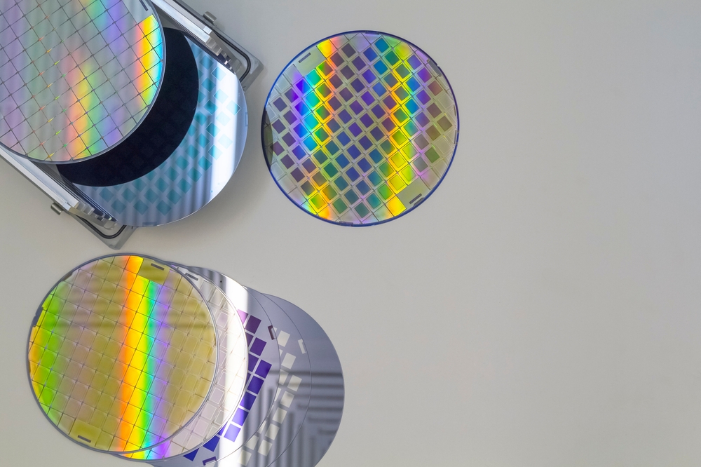
Wacker Chemie AG is to expand its capacity for cleaning semiconductor-grade polysilicon.
Accordingly, there are plans to set up a new production line at the company’s Burghausen site by early 2025. The new plant will increase existing capacity at the site by well over 50 percent. The etching of polysilicon chips is the crucial step in production to ensure the material surface purity required for semiconductor applications. Capital expenditures for the project are expected to exceed €300 million. This will create not only more than 100 new jobs at WACKER’s Burghausen site but also additional jobs at partner companies.
As well as expanding capacity, the project includes substantial capital expenditures for research and innovation. The aim here is to further increase the purity of polysilicon by means of new, highly automated processes, thus enabling semiconductors to meet even smaller design rules and making chips even more powerful. WACKER applied for funding for this part of the overall project under the EU’s Important Projects of Common European Interest (IPCEI) program. In this regard, the European Commission granted the necessary approval under state aid law on June 8, 2023. If the application is now approved by the German Ministry of Economic Affairs and Climate Protection, WACKER expects to receive funding of up to €46 million.
“As the only European producer of ultrapure polysilicon, we are proud to be making an important contribution to strengthening Europe’s microelectronics supply chain with this project,” explained WACKER CEO Christian Hartel. He went on to say that, at the same time, this investment project was an important part of WACKER’s strategy to intensify its focus on polysilicon for applications that demand extremely high quality. “By expanding our surface-cleaning capacity, we are creating the necessary conditions for meeting the continued fast-growing demand of our semiconductor customers. Thanks to this investment, we are also able to take the quality of our material to the next level so as to support the semiconductor sector’s latest technologies,” he added.
When the company introduced its new growth targets in March of last year, it announced that, in addition to producing material for solar cells with a particularly high efficiency, it would, going forward, expand its polysilicon capacity for semiconductor applications. WACKER POLYSILICON plans to double its sales with semiconductor-sector customers by 2030. It has earmarked investment of some €100 million for each of the next few years.
Cleaning the surface of the polysilicon chunks used as a starting material for making semiconductor wafers is a complex and technically very demanding process. Strong acids are used in an etching process to remove the uppermost layer from the surface of the polysilicon. The polysilicon is then packaged under cleanroom conditions for shipment to customers. The use of state-of-the-art technologies and a high degree of automation means that the new facilities achieve a surface purity that already meets the ever-greater demands required for future generations of semiconductor wafers.


