Accelovant achieves technology breakthroughs in Korea

Canadian-Korean collaboration successfully completes strategic technology development with global Korean semiconductor fabrication equipment suppliers.
Accelovant, a developer of fiber-optic sensing solutions for semiconductor, industrial, IoT, manufacturing, and power distribution markets, has completed a multi-year collaboration with several Korean semiconductor fabrication equipment suppliers to develop new fiber-optic sensing solutions that address next-generation performance of global semiconductor fabrication firms. The project is facilitated through Eureka, an international network for industrial research and development (R&D) collaboration that includes over 45 economies, and of which the National Research Council of Canada (NRC) is Canada’s National Office. Accelovant received advisory services and funding support from the NRC Industrial Research Assistance Program (NRC IRAP), while partners in Korea were supported through the Korea Institute for Advancement of Technology (KIAT).
Eureka is a network for market-driven industrial R&D that brings together governments, industry, research institutes, universities, and other innovation-focused organizations to raise the productivity and competitiveness of business through the development and commercialization of technology.
“The collaboration between Korean equipment manufacturers and Accelovant helps raise the performance, quality, and production capacity of semiconductor manufacturing facilities in Korea and around the world,” said Mr. WM Lee, chief executive officer of QSP, a key business partner of Accelovant. “The Korean semiconductor industry is well known for the speed in which it creates new process technologies. Through our Eureka collaboration project, Accelovant has contributed to advances that enable Korean fabrication equipment companies to achieve faster throughput, greater yields, and improved competitiveness.”
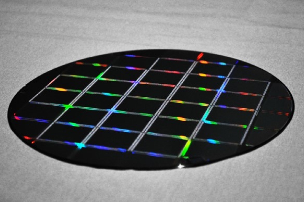
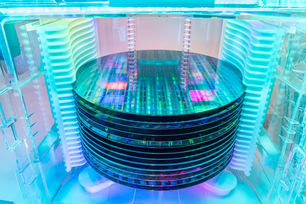
Accelovant’s focus for this initiative was to develop higher-accuracy sensors, able to operate over wider temperature ranges from minus 95 degrees Celsius to 450 degrees Celsius, and to allow users to significantly cut the cost per measurement point. These new sensors will support initiatives to increase process temperatures to enable faster production and more precise temperature control across wafers—a key factor in increasing yield per wafer.
“We are grateful to Eureka, the support received through NRC IRAP in Canada, and the KIAT team in Korea for facilitating this opportunity to work together with many of Korea’s leading semiconductor manufacturing equipment makers,” said Michael Goldstein, Accelovant chief executive officer. “Working with global leaders in this space not only provides our team with excellent advice and feedback, it also aids us in introducing our Canadian technology to a broad international marketplace. With the rapidly escalating private investment and government initiatives to accelerate semiconductor manufacturing in both Canada and the United States, such as the U.S. CHIPS and Science Act to build strategic capacity in the U.S., and Canada’s Semiconductor Action Plan, we anticipate a strong and immediate need for our new sensing technologies.”

