
D2S receives milestone order
D2S, a supplier of GPU-accelerated solutions for semiconductor manufacturing, has received a milestone order for its 50th GPU-accelerated computational design platform (CDP), a scalable processing solution for simulation-based semiconductor design and manufacturing applications.
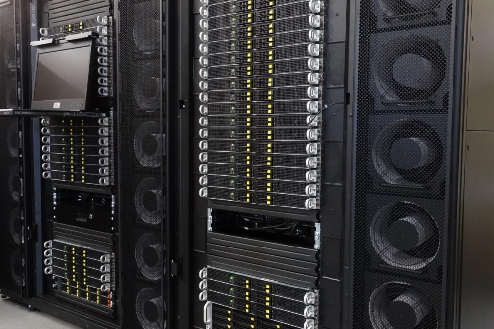
D2S CDPs are architected to ensure the high speed, accuracy and reliability required for 24x7 cleanroom production environments, and provide a variety of benefits to help customers achieve manufacturing success on their leading-edge photomask and chip designs. Altogether, D2S has incorporated more than 3,000 GPUs into its CDP products, representing a combined total of more than 50,000,000,000,000,000 floating point operations per second (50 PetaFLOPS) of single precision (SP) processing speed.
Last month, NVIDIA CEO Jensen Huang spoke at the ITF World 2023 semiconductor conference in Antwerp, Belgium, where he discussed the importance of accelerated computing and how GPUs are becoming increasingly integral to chip manufacturing. D2S was cited by Huang as an example of a company leveraging NVIDIA GPU accelerated solutions for advanced chip manufacturing.
GPU Acceleration Revolutionizing Semiconductor Design and Manufacturing
Computing applications used in semiconductor design and manufacturing have ever-increasing requirements for speed, accuracy and reliability as the leading-edge nodes – fueled by high-performance computing and artificial intelligence (specifically deep learning) – enter the 3-nm era and beyond. These applications include inverse lithography technology (ILT) to produce curvilinear shapes on photomasks, mask process correction (MPC) for multi-beam mask writing to process these incredibly complex mask shapes, curvilinear mask and wafer simulation and verification, and deep learning for photomask and semiconductor manufacturing.
Curvilinear mask features have been shown not only to print more accurately, but also to print more reliably, which is good for both mask and wafer quality. At the same time, leading-edge mask making is inherently pixel-based – from ILT that computes the desired mask shapes in the pixel domain in order to optimize wafer performance, including D2S TrueMask® ILT; and multi-beam mask writers that expose the resist on the mask using hundreds of thousands of eBeam pixels in parallel; to mask inspection and metrology systems, which take digitized (pixel-based) pictures to verify and monitor mask quality. The shift to the pixel domain for leading-edge masks naturally leads to the use of GPU-accelerated computing, which excels in pixel-domain computation. In addition, GPU-based computing is a foundation for most deep learning computations, which have become important for complex, computation-heavy applications.
D2S CDPs combined with D2S GPU-accelerated software solutions enable simulation-based accurate manipulation and analysis, particularly for curvilinear shapes. D2S software applications are based on NVIDIA CUDA, a parallel computing platform and programming model for GPUs. The latest seventh-generation CDP from D2S is powered by NVIDIA Ampere architecture-based A40 GPUs, and achieves more than 1.8 PetaFLOPS (SP) of computing power in a one-rack CDP.
According to Aki Fujimura, CEO of D2S, “D2S GPU-accelerated pixel-domain solutions help customers to achieve manufacturing success on their leading-edge mask and chip designs. Curvilinear mask making is now a practical reality thanks in part to GPU acceleration. Now that the mask manufacturing chain is ready for curvy, it’s time for the EDA infrastructure to rethink the Manhattan assumption of chip designs. With the power of GPU computing and the ability to manufacture curvy design features, the door is finally open for curvy design tools to enable even better manufacturing-aware designs.”


