
Increasing yield in chip production
Coronus DX builds on Lam's 15-year heritage of innovation in bevel solutions.
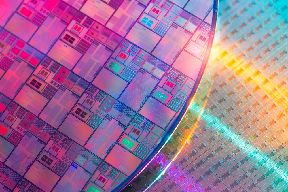
Lam Research Corp. has introduced Coronus DX, said to be the industry's first bevel deposition solution optimized to address key manufacturing challenges in next-generation logic, 3D NAND and advanced packaging applications. As semiconductors continue to scale, manufacturing becomes increasingly complex with hundreds of process steps needed to build nanometer-sized devices on a silicon wafer. In a single step, Coronus DX deposits a proprietary layer of protective film on both sides of the wafer edge that helps prevent defects and damage that can often occur during advanced semiconductor manufacturing. This powerful protection increases yield and enables chipmakers to implement new leading-edge processes for the production of next-generation chips. Coronus DX is the newest addition to the Coronus® product family and extends Lam's leadership in bevel technology.
"In the era of 3D chipmaking, production is complex and costly," said Sesha Varadarajan, senior vice present of the Global Products Group at Lam Research. "Building on Lam's expertise in bevel innovation, Coronus DX helps drive more predictable manufacturing and significantly higher yield, paving the way for adoption of advanced logic, packaging and 3D NAND production processes that weren't previously feasible."
Deposition Adds Critical Protection During Process Integration
Complementing Coronus bevel etch technology, Coronus DX is a game-changer for chipmakers by enabling new device structures. Repeated layers of processing can cause residues and roughness to accumulate along the wafer edge where they may flake off, drift to other areas, and create defects that cause a semiconductor device to fail. For example:
• In 3D packaging applications, material from back-end-of-line can migrate and become a contamination source in future processing. Roll-off in the wafer edge profile can impact wafer bonding quality.
• Long wet etch processes in 3D NAND manufacturing may result in severe substrate damage at the edge.
When those defects cannot be etched away, Coronus DX deposits a thin dielectric layer of protection on the bevel. This precise and tunable deposition helps resolve these common issues that may impact semiconductor quality.
"CEA-Leti applied its expertise in innovative, sustainable technology solutions to help Lam Research tackle key challenges in advanced semiconductor manufacturing," said Anne Roule, head of the Semiconductor Platform Division at CEA-Leti. "By simplifying 3D integration, Coronus DX drives significantly higher yield and enables chipmakers to adopt breakthrough production processes."
Proprietary Process Drives Yield Improvement
Coronus DX enables best-in-class precision wafer centering and process control, including integrated metrology, to ensure consistency and repeatability of the process. Coronus products incrementally increase wafer yield, delivering an additional 0.2 to 0.5 percent of yield per etch or deposition step, which can result in up to 5 percent improvement across the wafer flow. Manufacturers running more than 100,000 wafer starts per month may yield millions of extra die with Coronus – potentially worth millions of dollars – over the course of a year.
Every Major Chipmaker Uses Coronus
First introduced in 2007, the Coronus product line is used by every major semiconductor manufacturer, with several thousand chambers installed globally. Lam's Coronus product family is the industry's first mass production-proven bevel technology. Its Coronus and Coronus HP solutions are etch products designed to prevent defects by removing layers along the edge. Coronus solutions are used in the manufacturing of logic, memory and specialty devices, including leading-edge 3D devices. Coronus DX is now being used in high-volume manufacturing at leading customer fabs around the world.
"Improving quality in the production process through advancements in areas such as bevel technology is essential to our ability to provide next-generation flash memory at scale to our customers," said Hideshi Miyajima (Ph.D.), technology executive of Memory Process at Kioxia Corporation. "We look forward to continuing to work with Lam Research and its Coronus solutions to enable leading-edge wafer production."


