
Making the most of microscanners
The potential of micro scanners in medical technology is immense.
Their small size, low weight and high energy efficiency make them ideal for mobile use. More than 200 different micro scanner designs have been developed at Fraunhofer IPMS to meet customer-specific requirements. The range of services covers the entire value chain, from design and prototype development to pilot production in its own clean room on 8” wafer. Fraunhofer IPMS is continuously expanding the application range of scanner mirror technology with novel and patented design solutions and technology modules as well as the integration of artificial intelligence.
Micro scanners are tiny optical components that can deflect tiny mirrors around one or more axes to enable very fast and precise scanning or projection. Their non-contact operation, small size, low weight and high energy efficiency open up new possibilities in medical technology. Medical applications for micro scanners include image acquisition for medical endoscopes, confocal microscopy, fluorescence microscopy, spectroscopy and ophthalmology.
The micro scanners of Fraunhofer IPMS feature large scanning angles and high scanning frequencies, as well as excellent long-term stability. The institute's services also include supporting customers in the development of specific module setups and electronic solutions for controlled, high-precision actuation. For small and medium-sized companies in particular, the various evaluation kits from the Fraunhofer Institute offer the possibility of integrating micro scanner technology into their product development without the need for time-consuming and costly in-house development of control electronics to meet specifications.
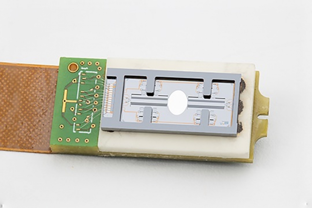
Application of Fraunhofer IPMS micro scanners in medical technology
In recent years, Fraunhofer IPMS has been able to qualify its previous customer-specific developments of micro scanners in order to be integrated into customer products. So these devices could prove their worth in praxis.
A few years ago, for example, Fraunhofer IPMS developed double-resonant MEMS scanners that form the core of a compact X-ray film scanner for digitalized dentistry. These micro scanners are qualified for the customer product in the in-house clean room as part of a pilot production of up to a few thousand units per year. Assembly onto a specially developed component carrier with integrated electronics and subsequent testing is also carried out at Fraunhofer IPMS. The institute's ISO 9001 certification guarantees that the Fraunhofer IPMS also focuses on quality according to industrial standards.
Other applications of Fraunhofer IPMS medical technology include the laser scanner development for the company Norlase that are used in ophthalmology to treat retinal and glaucoma patients. The use of MEMS scanners from the Fraunhofer IPMS makes it possible to achieve an unprecedented miniaturization of the system and a higher resolution.
For the start-up company Envision Diagnostics, the institute is developing micro scanners for a standardized, fast and reliable eye test that records, evaluates and displays all qualitative parameters. This will provide doctors with more comprehensive and reliable patient data, enabling them to make safer decisions.
Application of Fraunhofer IPMS micro scanners in microscopy
Micro scanning mirrors also have many applications in medical microscopy. Thanks to optical coherence tomography, the surface and depth structure of objects can be analyzed with a resolution in the micrometer range. Micro scanning mirrors from Fraunhofer IPMS enable a new type of recording of environmental parameters and are at the heart of a new type of laser scanning microscope for tumor delineation. This makes cancer surgery faster, more precise and safer. While still in the operating theatre, the surgeon can use the microscope to examine the tissue from which the tumor has just been removed. A fluorescent marker applied beforehand makes any cancer cells remaining after the incision visible. These can then be removed completely and precisely. The surrounding tissue is spared because the microscope display shows exactly where the healthy tissue begins. And there is no need to wait for laboratory results.
The ZEISS Lattice Lightsheet 7 from Zeiss, which was awarded the German Future Prize 2022 by the German President, also uses micro scanner technology from Fraunhofer IPMS. The microscope system for gentle 3D imaging of living cells uses, among other things, the Light Deflection Cube (LDC) scanner module developed by the institute. This has been qualified and is also made available to the customer Zeiss as part of a pilot production for the current product.


