Intel to sell minority stake in IMS Nanofabrication
Transaction will accelerate innovation of critical multi-beam mask writing tools, foster deeper cross-industry collaboration.
Intel has agreed to sell an approximately 20% stake in its IMS Nanofabrication GmbH business to Bain Capital Special Situations, in a transaction that values IMS at approximately $4.3 billion. The transaction is expected to close in the third quarter of 2023. IMS will operate as a standalone subsidiary and will continue to be led by CEO Dr. Elmar Platzgummer.
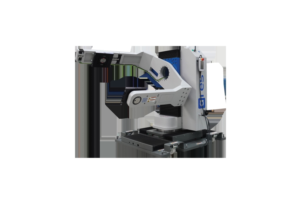
Since inventing multi e-beam technology and introducing the first commercial multi-beam mask writer in 2015, Vienna, Austria-based IMS has been an industry leader in multi-beam mask writing for advanced technology nodes. Intel initially invested in IMS in 2009 and ultimately acquired the business in 2015. Since the acquisition, IMS has delivered a significant return on investment to Intel while growing its workforce and production capacity by four times and delivering three additional product generations.
Today, as EUV technology becomes broadly adopted in leading-edge technologies, the multi-beam mask writing tools required to create advanced EUV (extreme ultraviolet lithography) masks are increasingly critical components to the semiconductor manufacturing ecosystem. This investment will position IMS to capture the significant market opportunity for multi-beam mask writing tools by accelerating innovation and enabling deeper cross-industry collaboration.
“The advancement of lithography is critical to driving continued progress in the semiconductor industry, and mask writing plays a central role in the industry’s transition to new patterning technologies, such as high-NA EUV,” said Matt Poirier, senior vice president of Corporate Development at Intel. “Bain Capital’s investment and partnership will provide IMS with increased independence and bring strategic perspective to help accelerate the next phase of lithography technology innovation, ultimately benefitting the ecosystem as a whole.”
Platzgummer said, “We are pleased to gain a valuable partner in Bain Capital, which has a long history of partnering with companies to drive growth and value creation. They share our conviction in the meaningful opportunity ahead for IMS as EUV becomes more pervasive and high-NA EUV moves from development into high-volume manufacturing in the second half of the decade. We look forward to expanding our ability to support the world’s largest chip producers, who rely on our technology to produce current and next generations of semiconductor products.”
Marvin Larbi-Yeboa, a partner at Bain Capital, said, “As the global leader and innovator of emerging technologies in the semiconductor fabrication and nanotech industries, we believe IMS is well-positioned to capitalize on attractive secular tailwinds as additional chip production capacity comes online and build on its leading competitive position, tech differentiation and cutting-edge product capabilities.”
Will Tetler, a managing director at Bain Capital, added, “We look forward to partnering with IMS’ exceptional management team and Intel to employ our deep industry experience and value-creation capabilities to support the business’ long-term growth strategy through further investment in its leading-edge tech and product portfolio to enable IMS to extend its competitive market position.”


