
How advanced cleaning helps achieve optimal wafer yields at advanced semiconductor nodes
With the introduction of SAPS and TEBO technology in a megasonic system,
semiconductor manufacturers now have new tools in their fight to
achieve optimal wafer yields.
By ACM Research.
Semiconductor chip features continue to shrink at a rapid pace. Dynamic random access memory (DRAM) manufacturers are now manufacturing 16GB chips in the 12nm range with an aspect ratio of 60:1 in the capacitor. NAND structures are reaching 232 layers with an even larger etch aspect ratio, and logic is moving into the first phase of gate-all-around (GAA) transistors at the 3nm node.
As these structures continue to shrink, the process technology becomes more challenging and removing contamination and random defects becomes extremely difficult. With minimum feature sizes and film thicknesses reaching the 10nm level (100 Ångstroms), a particle as small as 1nm (10Å) can be a killer defect causing a transistor not to function. Removing particles and other contaminants to reach acceptable yields in the manufacturing process will be one of the major process challenges for semiconductor manufacturers as chip features continue to shrink to below 10nm.
Wafer cleaning is sometimes considered low-tech in a semiconductor fab filled with advanced lithography, etch, and deposition equipment. However, the need to remove particles and other contamination that could change transistor characteristics, as well as contact and interconnect line resistance, has elevated wafer-cleaning technology to a higher level in the semiconductor manufacturing process. In fact, cleaning technology is now one of the most critical components of a semiconductor manufacturing line. In leading-edge factories, there can be more than 200 cleaning steps in the manufacturing process. Before each lithography process, thermal process, or deposition step, the wafer is typically cleaned to remove any defects and improve the material’s surface quality.
Cleaning systems have evolved beyond hand-operated dip-and-dunk systems, which use chemicals poured from bottles followed by a physical scrub/spray, as well as megasonic tank particle removal. Today’s systems comprise sophisticated process equipment that accurately measures out cleaning chemistries and removes microcontamination and defects after etch, lithography, chemical mechanical planarization (CMP), and other semiconductor manufacturing steps.
Conventional particle-removal cleaning is challenged by today’s advanced technologies’ smaller and finer features. The pressure levels needed when using a spray cleaning technology are too strong; the physical force will damage the surface features of the transistor and capacitor structures, potentially knocking them off the wafer. Spray technology also cannot reach into the trenches with deep aspect ratios.
Conventional megasonic cleaning also struggles with the small, deep features, as the energy cannot reach deep into the structures evenly. Conventional megasonics cannot guarantee even surface coverage across the wafer, which often results in insufficient cleaning in some wafer areas. This leads to yield loss. These processes can also create surface roughness and material loss, which could significantly impact advanced device performance when 1 Å is crucial for chip performance. Essentially, megasonic wafer cleaning and conventional cleaning approaches have reached their limits and can no longer remove the smallest killer defects without damaging the features on the chip.
Removing particles from today’s patterned semiconductor is becoming a focused science. As chip features continue to shrink and move into the third dimension, the brute-force cleans using brush scrubbers and spray scrubbers, ultrasonics, and megasonic energy are evolving to avoid damaging the structures. New single-wafer cleaning process technologies address the critical nature of cleaning the current and next generation of patterned structures on the semiconductor chip.
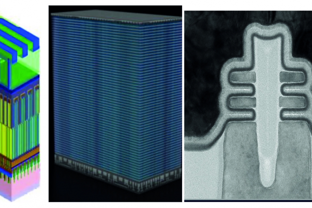
Main image: Figure 1. Advanced Process Technology DRAM cell, NAND structure, and forksheet transistor (Source Micron Technology Day, IMEC)
The NEXT generation cleaning technology
To address the cleaning challenges facing semiconductor equipment manufacturers, ACM Research developed Smart Megasonix™—a smarter, more innovative suite of single-wafer wet cleaning technologies that can be used at existing and future process nodes across the range of processing steps to achieve more thorough, comprehensive cleaning without damage to device features. These proprietary technologies can control both the power intensity and the distribution of megasonic cleaning.
Two key technologies have been introduced to enhance the cleaning abilities of megasonic systems. The first is Space Alternated Phase Shift (SAPS™) wafer cleaning technology. The SAPS technology is an advanced megasonic process that uses alternating phases of megasonic waves in the gap between the megasonic transducer and the wafer. The SAPS technology moves or tilts the transducer while the wafer rotates, delivering megasonic energy uniformly across all points on the wafer, even if the wafer is warped. This ensures optimum energy delivery, which, when combined with the proper dilute chemistry, creates the right environment for removing wafer defects. The precision of the SAPS technology enhances the mass transfer rate of dislodged defects and improves efficiency of the system’s particle removal. Implementing SAPS results in faster throughput and more efficient particle removal, which translates to higher yield as well as lower wafer cost of ownership.
The second innovative development in megasonic technology is Timely Energized Bubble Oscillation (TEBO™). Conventional megasonics use cavitation to generate bubbles that are the active cleaning energy. In a conventional system, these bubbles can implode or collapse, which can then damage finely patterned features. With TEBO, the cavitations become stable without bubble implosion or collapse. The result is successful defect removal without damage to sensitive patterns such as high-aspect-ratio capacitors in DRAM and high-aspect-ratio trenches and holes in 3D NAND. The technology also removes defects from advanced fin field-effect transistor (FinFET) and GAA structures.
As chip features shrink and aspect ratios increase, removing etch and photoresist residue as well as CMP particles becomes more challenging. Features are more fragile, and the atomic forces causing the defects to adhere to the wafer are significantly stronger. New clean chemistries and mechanical methods for defect removal that do not damage critical features are needed for advanced processing. With the introduction of SAPS and TEBO technology in a megasonic system, semiconductor manufacturers now have new tools in their fight to achieve optimal wafer yields.
New single-wafer cleaning process technologies address the critical nature of cleaning the current and next generation of patterned structures on the semiconductor chip.


