
Samsung Electronics unveils Foundry Vision
Samsung further solidifies foundry leadership and customer commitment with advanced process roadmap.
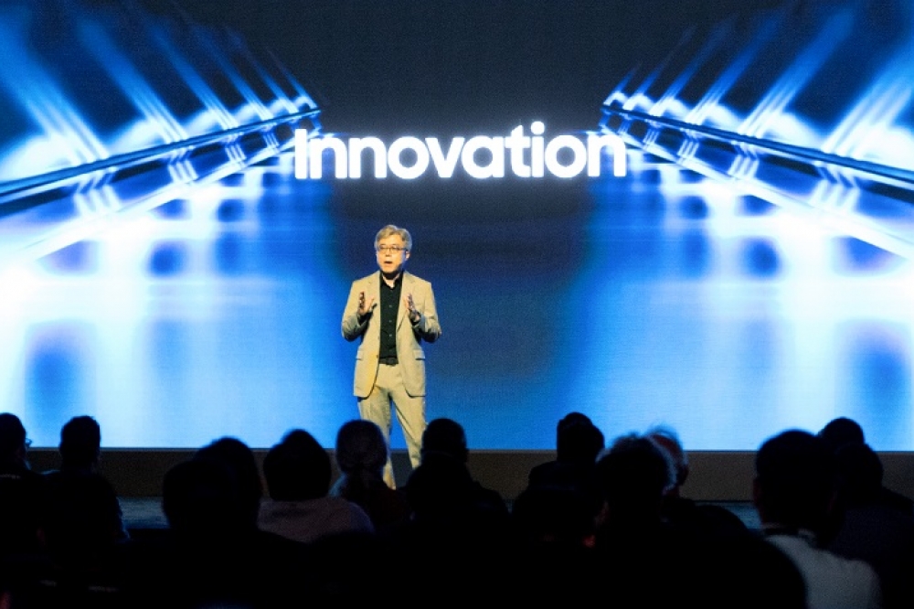
Samsung Electronics has announced its latest foundry technology innovations and business strategy at the 7th annual Samsung Foundry Forum (SFF) 2023.
Under the theme “Innovation Beyond Boundaries,” this year’s forum delved into Samsung Foundry’s mission to address customer needs in the artificial intelligence (AI) era through advanced semiconductor technology.
Over 700 guests, from customers and partners of Samsung Foundry, attended this year’s event, of which 38 companies hosted their own booths to share the latest technology trends in the foundry industry.
“Samsung Foundry has always met customer needs by being ahead of the technology innovation curve, and today, we are confident that our gate-all-around (GAA)-based advanced node technology will be instrumental in supporting the needs of our customers using AI applications,” said Dr. Siyoung Choi, President and Head of Foundry Business at Samsung Electronics. “Ensuring the success of our customers is the most central value to our foundry services.”
As part of its business strategy to solidify its competitiveness as a leading foundry service, Samsung Foundry today announced the following:
• Expanded applications of its 2-nanometer (nm) process and specialty process
• Expanded production capacity at its Pyeongtaek fab Line 3 (P3)
• Launched a new “Multi-Die Integration (MDI) Alliance” for next-generation packaging technology
• Continued progress in the foundry ecosystem with Samsung Advanced Foundry Ecosystem (SAFE™) partners
At the event, Samsung announced detailed plans for the mass production of its 2nm process, as well as performance levels.
The company will begin mass production of the 2nm process for mobile applications in 2025, then expand to HPC in 2026 and automotive in 2027. Samsung’s 2nm process (SF2) has shown a 12% increase in performance, a 25% increase in power efficiency and a 5% decrease in area, when compared to its 3nm process (SF3).
Mass production of SF1.4 will begin in 2027 as planned.
From 2025, Samsung will begin foundry services for 8-inch gallium nitride (GaN) power semiconductors targeting consumer, data center and automotive applications.
To secure the most cutting-edge technology in 6G, the 5nm Radio Frequency (RF) is also under development and will be available in the first half of 2025. Samsung’s 5nm RF process shows a 40% increase in power efficiency and a 50% decrease in area compared to the previous 14nm process.
In addition, the company will add automotive applications to its 8nm and 14nm RF, expanding beyond the mobile applications currently under mass production.
Under the “Shell-First” operation strategy that aims to better respond to customer demands, Samsung Foundry is maintaining its commitment to invest and build capacity by adding new manufacturing lines in Pyeongtaek, South Korea, and Taylor, Texas. Current expansion plans will increase the company’s clean room capacity by 7.3 times by 2027 compared to 2021.
The company plans to begin mass production of foundry products for mobile and other applications at Pyeongtaek Line 3 in the second half of the year. Samsung is also focusing on increasing its manufacturing capacity in the United States. Construction of the new fab in Taylor is proceeding according to initial plans and is expected to finish by the end of the year, beginning operation in the second half of 2024.
Samsung will continue to expand its production base to Yongin, South Korea, to power the next generation of Samsung’s foundry services. Yongin is a nearby city located about 10km east of Samsung’s Hwaseong and Giheung campuses.
In a bid to address the rapid growth in the chiplet market for mobile and HPC applications, Samsung is launching the MDI Alliance in collaboration with its partner companies as well as major players in memory, substrate packaging and testing.
The MDI Alliance leads innovation in stacking technology by forming a packaging technology ecosystem for 2.5D and 3D Heterogeneous Integration. Together with partners across the ecosystem, Samsung will provide a one-stop turnkey service to better support customers’ technological innovation.
Samsung plans to actively respond to customer and market needs by developing customized packaging solutions that are tailored to the individual needs of various applications including HPC and automotive.
Following the Samsung Foundry Forum, Samsung hosted the Samsung Advanced Foundry Ecosystem (SAFE™) Forum on June 28 under the theme “Accelerating the Speed of Innovation.”
Together with over a hundred partners across electronic design automation (EDA), design solution partners (DSP), outsourced semiconductor assembly and test (OSAT), cloud and IP, Samsung is promoting mutual growth of the foundry ecosystem to power the success of customers.
Samsung has long supported stronger collaboration between partners across the foundry ecosystem, advancing the boundaries of design infrastructure from 8-inch to the latest GAA process. Samsung and its 23 EDA partners now offer over 80 design tools and is also collaborating with 10 OSAT partners to develop 2.5D/3D packaging design solutions.
Samsung provides product design services to a variety of customers from startups to industry leaders through strong partnerships with nine DSP partners that have extensive expertise in Samsung Foundry processes, as well as nine Cloud partners.
Samsung has also secured a portfolio of over 4,500 key IPs from 50 global IP partners. Samsung plans to secure additional next-generation high-speed interface IPs for SF2, including LPDDR5x, HBM3P, PCIe Gen6 and 112G SerDes. Its long-term partnerships with leading global IP providers in their respective fields will help cater to customer needs in AI, HPC and automotive.
“Through extensive collaboration with our SAFE™ partners, Samsung Foundry is helping simplify designs that are becoming even more complex amid the application of the most advanced processes and new technologies such as heterogeneous integration,” said Jong-wook Kye, Executive Vice President and Head of Design Platform Development, Foundry Business at Samsung Electronics. “We will continue to strive for consistent growth in the Samsung Foundry ecosystem in terms of both scale and quality.”
Samsung Electronics will be hosting the Samsung Foundry Forum 2023 in South Korea in July, and the event will expand to Europe and Asia later in the year to meet customers in each region.


