
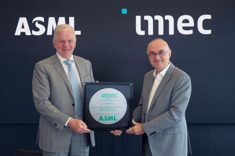
Imec and ASML sign MoU
ASML is making a substantial commitment in imec's future state-of-the-art pilot line.
Imec and ASML Holding intend to intensify their collaboration in the next phase of developing a state-of-the-art high-numerical aperture (High-NA) extreme ultraviolet (EUV) lithography pilot line at imec.
The pilot line is intended to help the industries using semiconductor technologies to understand the opportunities that advanced semiconductor technology can bring and have access to a prototyping platform that will support their innovations. The collaboration between imec, ASML and other partners will enable the exploration of novel semiconductor applications, the potential development of sustainable, leading-edge manufacturing solutions for chip makers and end users, as well as the development of advanced holistic patterning flows in collaboration with the equipment and material ecosystem.
The Memorandum of Understanding signed recently includes the installment and service of ASML’s full suite of advanced lithography and metrology equipment in the imec pilot line in Leuven, Belgium, such as the latest model 0.55 NA EUV (TWINSCAN EXE:5200), latest models 0.33 NA EUV (TWINSCAN NXE:3800), DUV immersion (TWINSCAN NXT:2100i), Yieldstar optical metrology and HMI multi-beam. The intended engagement represents a very significant value in the advanced pilot line.
This groundbreaking new High-NA technology is crucial for developing high-performance energy-efficient chips, such as next-generation AI systems. It also enables innovative deep-tech solutions that could be used to tackle some of the major challenges our society is facing in for instance healthcare, nutrition, mobility/automotive, climate change and sustainable energy. Significant investments are needed to secure industry-broad access to High-NA EUV lithography beyond 2025 and retain the related advanced node process R&D capabilities in Europe.
This Memorandum of Understanding kickstarts the next phase of intensive collaboration between ASML and imec on High-NA EUV. The first phase of process research is being executed in the joint imec-ASML High-NA lab using the first High-NA EUV scanner (TWINSCAN EXE:5000). Imec and ASML collaborate with all leading-edge chipmakers and materials and equipment ecosystem partners, with the goal to prepare the technology for the fastest possible adoption in mass manufacturing. In the next phase, these activities will be ramped up in the imec pilot line in Leuven (Belgium) on the next-generation High-NA EUV scanner (TWINSCAN EXE:5200).
The intensified collaboration plans on lithography and metrology technology between the two semiconductor players are in line with the ambitions and plans of the European Commission and its member states (Chips Act, IPCEI) in order to strengthen innovation to tackle societal challenges. Part of the collaboration between imec and ASML is therefore captured in an IPCEI proposal which is currently in review by the Dutch government.
“ASML is making a substantial commitment in imec's state-of-the-art pilot fab to support semiconductor research and sustainable innovation in Europe. As artificial intelligence (AI) rapidly expands into domains such as natural language processing, computer vision and autonomous systems, the complexity of tasks escalates. Therefore, it is crucial to develop chip technology that can meet these computational demands without depleting the planet's precious (energy) resources,” said Peter Wennink, President and Chief Executive Officer of ASML.
“This commitment from ASML, which builds on over 30 years of successful collaboration, sends a powerful signal of our unwavering dedication to drive the advancement of sub-nanometer chip technology,” commented Luc Van den hove, President and Chief Executive Officer of imec. “This collaboration serves as a testament to the strength that lies in unity within the chip industry. While these projects enable us to fortify our regional strengths initially, they also pave the way for future global cooperation, allowing partners worldwide to benefit from local breakthroughs. It is through these collective efforts that we can truly accelerate innovation and propel the semiconductor industry to new heights.”


