Siemens extends support for Samsung

Siemens Digital Industries Software has announced a range of new certifications and collaborations with longtime partner Samsung Foundry.
“Samsung Foundry is pleased to work closely with Siemens, which continues to increase its value to the Samsung Foundry ecosystem by offering more features in support of our latest processes,” said Sei Seung Yoon, Executive Vice President and head of Foundry Design Enablement team at Samsung Electronics. “Siemens has been a strong partner for many years, and we continue to further grow our strong and highly-valued partnership in helping our mutual customers bring to market compelling new IC innovations.”
Notable Siemens highlights and product certifications for Samsung Foundry’s advanced processes include:
Siemens’ Calibre platform
Siemens’ Calibre® nmPlatform software for integrated circuit (IC) verification sign-off is now fully certified for Samsung Foundry’s latest 3nm process technologies, and enablement activities for Samsung Foundry’s 2nm process are currently underway. The Calibre nmPlatform tools include: Calibre® nmDRC software, Calibre® YieldEnhancer™ software, Calibre® PERC™ software, Calibre® xACT™ software and Calibre® nmLVS software. In addition, Samsung recently introduced second-generation gate-all-around (GAA) transistors that continue to help improve performance, power and area (PPA) for designs. The Calibre xACT team partnered with Samsung Foundry to enhance existing Calibre xACT software functionality to support these new processes with a combination of field solver and table-based techniques for high attofarad-level precision and high performance that help customers achieve the accuracy and throughput required for parasitic extraction flows.
Siemens’ Analog FastSPICE platform
Siemens’ recent efforts to qualify its Analog FastSPICE (AFS) platform for Samsung Foundry’s advanced processes have met with significant success. Siemens’ AFS platform is now certified across Samsung Foundry’s fin field-effect transistor (FinFET), extreme ultraviolet (EUV) and GAA fabrication processes, namely 14LPP, 14LPU, 11LPP, 8LPP, SF4, SF4P, SF3 and SF3P. AFS is also qualified for Samsung Foundry’s fully depleted-silicon on insulator (FD-SOI) 18FDS process technology. With these certifications, mutual customers can now verify their designs using Siemens’ AFS platform with confidence and SPICE accuracy. Powered by Siemens’ Analog FastSPICE eXTreme™ platform, Siemens’ AFS platform provides leading-edge circuit verification for nanometer-scale designs with mixed-signal and variation-aware capabilities providing competitive performance, capacity and functionality.
Samsung Foundry and Siemens have also continued their active partnership in open model interface (OMI) development with Si2’s Compact Model Coalition (CMC). OMI, the industry-standard platform for enabling aging modeling and reliability analyses, is now supported by the AFS platform across the majority of Samsung Foundry’s processes from 14nm to 3nm.
Siemens’ Aprisa solution for place-and-route
Samsung and Siemens have completed qualification of the Aprisa™ solution for Samsung Foundry’s 5nm process technologies. Aprisa technology files for SF5 are available immediately from Samsung Foundry. This successful collaboration has resulted in an Aprisa digital implementation solution that supports all elements of Samsung Foundry’s 5nm methodology and design rules. To achieve this milestone, the Aprisa solution passed all Samsung requirements for DRC/LVS/DFM closure and timing/power closure, as well as correlation with signoff RC and STA, and the Calibre platform’s DRC/DFM functionality. The Aprisa solution offers comprehensive hierarchical and block level physical implementation solutions. The innovative detail-route-centric technology that powers the Aprisa software tool is ideal for a variety of IC designs at advanced and mature process nodes.
Siemens’ Tessent Multi-die software for 3D IC Test
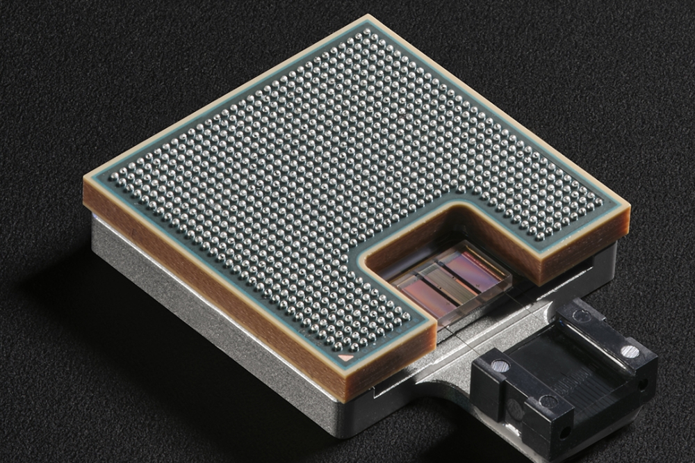
Siemens and Samsung have successfully demonstrated a consolidated Design for Test (DFT) flow using Siemens’ Tessent™ Multi-die software for 3D IC designs. The Tessent Multi-die solution inserts the required IEEE 1838 Primary Test Access Port (PTAP) and Secondary Test Access Port (STAP) for serial communication to the dies on the 3D stack. Siemens’ Tessent™ Streaming Scan Network software for its Tessent™ TestKompress™ software augments as the Flexible Parallel Port (FPP) of the IEEE 1838 standard. Samsung can now provide its customers with a 3D IC DFT reference flow that builds on established Tessent products and introduces new functionality to test and diagnose the stacked dies in the package. The Tessent Multi-die solution helps enable IEEE 1838-compliant DFT methodologies and extends proven 2D IC solutions to 3D IC applications.
“In certifying a broad range of Siemens’ leading toolsets for the foundry’s latest, most advanced processes, Samsung and Siemens are collaborating to help mutual customers meet aggressive time-to-market metrics,” said Joe Sawicki, executive vice president, IC-EDA for Siemens Digital Industries Software. “Once again, the combined expertise of Samsung and Siemens EDA has provided the global IC design community with solutions needed for creating and quickly validating ICs targeting multiple high-growth markets and applications.”
In addition to these process technology certifications, Siemens and Samsung are closely collaborating on a range of other initiatives for the benefit of mutual customers, including:
Samsung and Siemens worked to develop circuit reliability solutions that meet designers’ needs for circuit robustness in the areas of electrostatic discharge (ESD) and latch-up (LUP). These Calibre PERC topology checks are now mandatory for designs manufactured at Samsung’s 28nm node and below. Siemens and Samsung have also enhanced CPU scaling techniques to keep turnaround time (TAT) in check for customers, even as designs continue to grow in size and complexity.
Samsung and Siemens continue to collaborate on utilizing AI-powered technology for brute-force accurate high-sigma verification and characterization of standard cells and memories, using Solido™ Variation Designer software and Solido™ software for characterization. In addition, Siemens’ Solido Crosscheck software provides a repeatable and scalable platform for library PDK quality assurance. Together, these technologies in Solido enable high quality IP production for customer designs leveraging Samsung’s advanced process nodes, including 7nm to the latest 3nm technologies.
As connectivity and sensor content increases in leading-edge designs, demand is growing for comprehensive electromigration (EM) and voltage (IR) drop analysis solutions that scale to support even the largest of analog, mixed-signal and digital IC designs. Siemens’ mPower™ software offers high-capacity and high-performance power integrity analysis capabilities to address this need. Siemens is partnering with Samsung Foundry to enable Samsung customers to take advantage of the unique capability of the mPower software on Samsung’s 14nm process technologies and below.
As automotive ICs integrate more safety and security content with every new device generation, demand grows for smart new approaches to protecting this onboard content. One such approach is deployment of “safety islands”, which can help to secure automotive ICs from cyber threats such as remote access hacking. Safety islands manage and monitor the safety content within the SoC, to enable recovery of complex issues within the chip and signal failures to external systems, and also to be adaptable and upgradable for future needs and use cases. To learn more about how Siemens and Samsung Foundry are collaborating on safety island technology, make plans to attend the following session during Samsung Advanced Foundry Ecosystem (SAFE) Forum North America 2023 -- June 28th, 2023 at 2:55pm PDT: “Automotive Safety Island – An In-Life Solution to Managing Safety, Reliability, and Security for Modern Automotive ICs”.


