Speedier (S)TEM
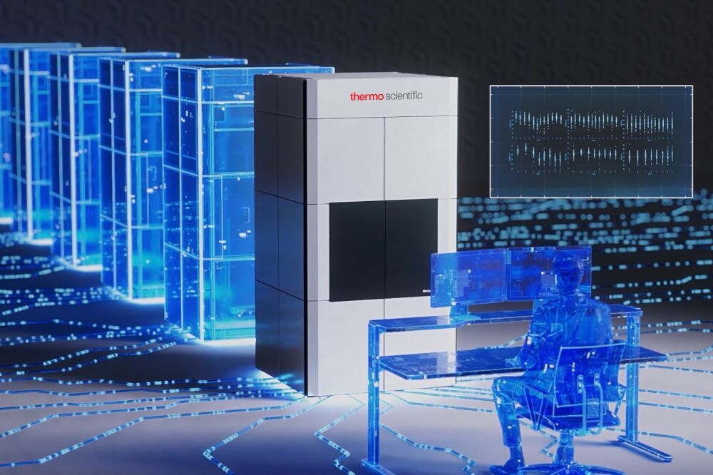
Thermo Scientific Metrios 6 Scanning Transmission Electron Microscope ((S)TEM) is designed to meet an industry need for faster access to large-volume, high-quality data; newly designed hardware and advanced machine learning techniques aim to optimize performance and reduce operating expenses.
Thermo Fisher Scientific has introduced the Thermo Scientific™ Metrios™ 6 Scanning Transmission Electron Microscope ((S)TEM) — a new-generation, fully automated (S)TEM metrology solution designed to help enhance productivity and deliver data quality assurance for high-volume semiconductor manufacturing.
The Metrios 6 (S)TEM enables fully automated TEM metrology and characterization workflows with up to 20% in average productivity improvement compared to the previous generation of the Thermo Scientific Metrios (S)TEM.
The more complex the semiconductor device 3D architecture, the more exact the in-depth metrology and characterization processes must be. As a proven leader in high-impact innovation, Thermo Fisher sees firsthand that the atomic-scale 3D intricacies in today’s devices are driving a need for a highly automated (S)TEM platform to enable faster access to large-volume, high-quality data and help accelerate learning cycles.
Built to increase productivity and accelerate data acquisition—therefore facilitating yield improvements and reducing time-to-market—the Metrios 6 (S)TEM incorporates industry-leading hardware and machine-learning algorithms to obtain large-volume high-quality data from complex devices and novel materials rapidly.
“Manufacturing semiconductors in today’s increasingly complex technological landscape demands not only high throughput and resource optimization, but also a larger volume of TEM data than ever before," said Mohan Iyer, vice president and general manager, semiconductor, at Thermo Fisher Scientific. "To address these challenges, we are proud to introduce the Metrios 6 automated (S)TEM metrology solution that boosts productivity through innovative hardware advancements and powerful software enhancements. With the Metrios 6 microscope, semiconductor manufacturers can now access actionable data faster, while simultaneously increasing tool and human resource productivity, thus accelerating semiconductor development cycles."
New features and capabilities compared to previous Metrios generations include:
• Smart Stage fully automated sample insertion and retraction mechanism eliminates manual operation and potential for human errors, enabling customers to perform high-resolution imaging at a faster pace.
• New Thermo Scientific Ultra-X EDS detection system offers fast compositional characterization and elemental mapping to ease challenging analysis on the most beam-sensitive materials and enable at least two times faster data collection.
• Newly designed objective lens and source innovations enable voltage switching in minutes versus hours, higher-efficiency (S)TEM and EDS acquisition and uncompromised resolution.
• Machine-learning-enabled automation eliminates tedious recipe generation for routine (S)TEM analysis and provides automated workflows with flexibility to generate large volume data without using highly skilled operators.


