
First non-destructive, in-line subsurface metrology system?
AUDIRA will complement current metrology techniques by providing highly accurate and non-destructive nanometer-level measurements through opaque layers of advanced leading-edge node devices.
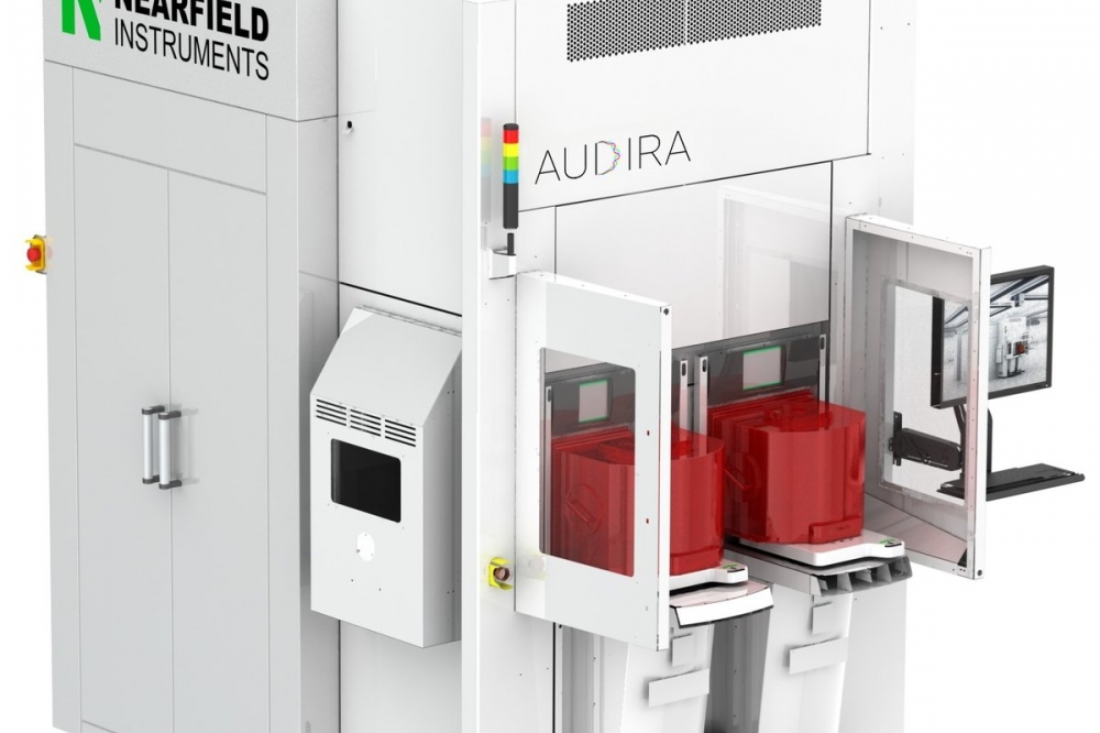
Nearfield Instruments has launched AUDIRA™ – said to be the industry’s first and only in-line, non-destructive subsurface metrology system for advanced semiconductor manufacturing. The AUDIRA system provides highly accurate and reproducible nanometer-level measurements of buried features and defects, such as voids, in advanced memory and logic devices.
“AUDIRA is a game-changer for advanced semiconductor manufacturing. It provides measurement data that was previously not available without having to remove the wafer from the line,” said Hamed Sadeghian, CEO, Nearfield Instruments. “Most importantly, the AUDIRA gives process engineers insight into the wafer’s innermost layers – details they never were able to measure before nondestructively and sometimes would never have even known to look for. AUDIRA, like our first product QUADRA™, turns in-line metrology and inspection into an added value in the semiconductor manufacturing process.”
Nearfield Instruments anticipates that AUDIRA will complement transmission electron microscopy (TEM) and critical dimension-scanning electron microscopy (CD-SEM) for subsurface process control measurements. AUDIRA uses an acoustic approach that is fast, very precise and non-destructive with the added advantages of being in-line with a fast turn-around time.
With AUDIRA, Nearfield Instruments combines an acoustic microscopy technique with its own proprietary atomic force microscopy (AFM) technology. The AFM probe is used to ‘listen’ to the sound waves coming through the wafer layers. The wave interacts with all the transitions and surfaces within the device and reflects information back. The pattern of that reflected wave and the time of arrival contains data about the structure below the surface. The AUDIRA scans across the die, with each step as small as several tenths of a nanometer. The data is then translated into a comprehensive pattern of the underlying layers that provides measurement of subsurface features.
AUDIRA is also valuable for measuring shallow features through the surface. Using the AFM probe, surface elasticity variations can be quickly measured to reveal details about the structure below. Nearfield Instruments works with customers to develop a recipe for when to use acoustics and at what frequency, for which layers local elasticity measurements are best, and when to switch to wave propagation schemes.
Nearfield Instruments’ product portfolio also includes the QUADRA™ surface metrology solution. It features a groundbreaking multi-miniaturized AFM head architecture combined with feedforward trajectory planner (FFTP) imaging technology to enable on-device, non-destructive measurements for in-line process monitoring of very high-aspect ratio structures as well as hybrid bonding and EUV resist critical dimension metrology. QUADRA has shown a factor of more than 100x improvement in imaging acquisition time when benchmarked against existing state-of-the-art AFM systems.
AUDIRA is available for ordering now and the first systems will ship in Q2 2024 to top semiconductor fabs worldwide.


