Mersen opens manufacturing facility
Further graphite production capacities scheduled as part of the Group’s 2027 plan Start-up of isostatic graphite production, mainly for the semiconductor market.
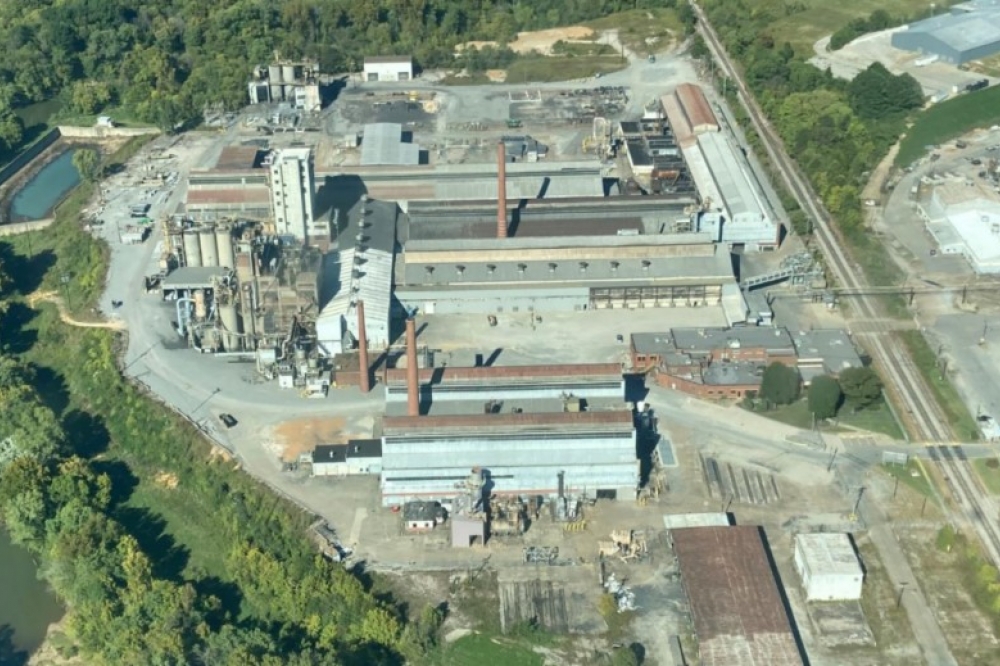
Mersen, a global expert in electrical power and advanced materials, has officially opened its new manufacturing facility this afternoon, located at 795 Santa Fe Pike in Columbia, TN. The Maury County facility will be the global manufacturer's 10th U.S. location.
Mersen has invested $70 million in the Tennessee facility and plans to invest more over the next 1-3 years including $25 - $30 million in 2023 and has hired nearly 100 employees from the region, with plans to hire 50 more in the next 12 months.
The Columbia, TN location is considered a multi-activity center of excellence that will strengthen our industrial capabilities and allow us to ramp-up several high-growth markets like solar power and electronics. This location will focus on the manufacturing of extruded graphite, insulation felt and isostatic graphite that will be used for green technology products used in solar panels, semiconductors and electric vehicles.
“I am thrilled to join Columbia in welcoming Mersen to Maury County," said Tennessee Congressman Andy Ogles. "Their investment in our community, from repurposing a local facility to creating jobs for Tennesseans, is inspiring. I look forward to seeing its continued growth going forward. Manufacturing plays an integral part in the lives of so many of us. I trust that Mersen and its innovative technology will bring countless opportunities to Middle Tennessee in the years to come.”
The Mersen team strategically renovated the industrial site that was once home to Union Carbide and Graftech Advanced Graphite. After acquiring the plant in July 2019, Mersen has invested millions to reshape, rehabilitate and re-industrialize the site to match the group’s industrial requirements and accelerate its development in its key markets. The plant will quickly have the capacity to produce 4,000 tons of extruded graphite, 120 tons of insulation felt, and 2,000 tons of isostatic graphite per year.
As part of its 2027 strategic plan, Mersen will further increase its isostatic graphite manufacturing capacities to reach 4,000 tons in Columbia by the end of 2024. The Columbia site’s configuration means it could accommodate other production capacities in the future, if required.
“I’m very proud of what has been achieved at the Columbia site in the last four years, in terms of redevelopment, investment, production start-up and more,” said Luc Themelin, Mersen’s Chief Executive Officer. “It is now a key site in our manufacturing base, bringing together production capacities for extruded graphite, isostatic graphite and insulating felts. This important strengthening of our industrial capacities will enable us to achieve the objectives of our 2027 plan, and we intend to continue investing to meet increased demand from sustainable development markets, particularly the SiC semiconductor market.”


