+44 (0)24 7671 8970
More publications     •     Advertise with us     •     Contact us
 
Loading...
News Article

Applied Materials and Fraunhofer IPMS launch European Semiconductor- Metrology Technology Hub

News

New hub will provide state-of-the-art metrology systems to accelerate semiconductor research and enhance development projects with chipmakers and ecosystem partners across Europe, particularly in ICAPS market segments.

Applied Materials and the Fraunhofer Institute for Photonic Microsystems IPMS have revealed a landmark collaboration to create Europe´s largest technology hub for semiconductor metrology and process analysis.


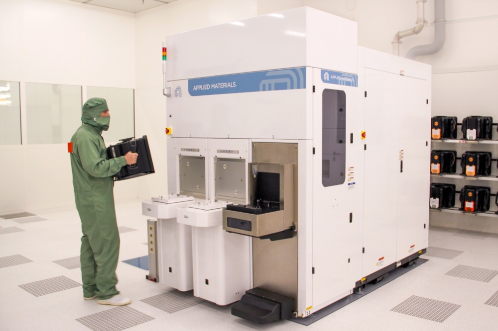
To be located at the Center Nanoelectronic Technologies (CNT) of Fraunhofer IPMS in Dresden, the technology hub is situated in the heart of Silicon Saxony, Europe’s largest semiconductor cluster. The hub will be equipped with Applied Materials’ state-of-the-art eBeam metrology equipment, including its VeritySEM® CD-SEM (critical dimension scanning electron microscope) systems, and staffed by Applied engineers and R&D experts.


“Fraunhofer IPMS and its partners will benefit from access to Applied’s industry-leading eBeam metrology systems”, said Dr. Benjamin Uhlig-Lilienthal, Head of Business Unit Next Generation Computing at Fraunhofer IPMS. “The new technology hub will offer advanced wafer-level metrology in our industrial CMOS environment with Fraunhofer IPMS’s unique ability to loop wafers directly with semiconductor manufacturers.”


“Our collaborative metrology hub will accelerate learning cycles and the development of new applications for the Fraunhofer Institute, Applied Materials and our customers and partners in Europe,” said James Robson, Corporate Vice President for Applied Materials Europe. “This unique technology hub will have the capability to test and qualify processes on a variety of substrate materials and wafer thicknesses critical to applications across the diverse European semiconductor landscape.”


Metrology is crucial in the production of microchips as it enables the accurate measurements needed to precisely monitor and control the quality of individual semiconductor manufacturing steps and sequences. Chipmakers use metrology equipment at critical points to help validate physical and electrical characteristics and maintain target yields.

Reality AI Explorer Tier offers free AI/ML development access
AEM introduces new generation of Automated Burn-In Systems
NPUs are emerging as the main rival to Nvidia’s AI dominance, says DAI Magister
Camtek receives a $20M order from a Tier-1 OSAT
Free samples of every STMicroelectronics NPI IC available from Anglia
NY CREATES and SEMI sign MoU
Major government investment to 'propel' Canada
QuickLogic announces $5.26 million contract award
ASNA and Athinia collaborate
Global sales forecast to reach record $109 billion in 2024
AMD to acquire Silo AI
Nanotronics unveils 'groundbreaking' Gen V AI Model
Aitomatic unveils SemiKong
Biden-Harris Administration reveals first CHIPS for America R&D facilities and selection processes
Collaboration to produce cutting-edge AI accelerator chips
Oxford Ionics breaks global quantum performance records
Adeia wins ECTC Award for paper on “Fine Pitch Die-to-Wafer Hybrid Bonding”
AEM introduces new generation of Automated Burn-In Systems
Sydney council forges vital semiconductor agreement
EV Group's EVG880 LayerRelease wins 2024 Best of West
Biden-Harris Administration to invest up to $1.6 billion
Cyient sets up subsidiary for semiconductor business
EMD Electronics network leaders honoured
Accenture acquires Cientra
Introducing Park FX200
Deep learning chipset market to surge to $72.8 billion by 2033
PI Innovation Award 2024: Nanobodies for Diagnostic and Therapeutic Applications
Graphcore joins Softbank Group
Kaman Measuring highlights high precision displacement sensors
Si2 reveals recipients of Annual Power of Partnerships Award
Advantest achieves ASPICE Level 2 Certification for V93000 SmarTest 8 Software
Semiconductors to become a trillion-dollar industry by 2030
×
Search the news archive

To close this popup you can press escape or click the close icon.
Logo
×
  • 1st January 1970
  • 1st January 1970
  • 1st January 1970
  • 1st January 1970
  • 1st January 1970
  • 1st January 1970
  • 1st January 1970
  • 1st January 1970
  • View all news 22645 more articles
Logo
×
Register - Step 1

You may choose to subscribe to the Silicon Semiconductor Magazine, the Silicon Semiconductor Newsletter, or both. You may also request additional information if required, before submitting your application.


Please subscribe me to:


You chose the industry type of "Other"

Please enter the industry that you work in: