$2 billion factory for Singapore

Silicon Box has launched what it says is the world’s most advanced semiconductor factory in Singapore, positioning the country as a global leader in high-performance technology.
Silicon Box, a Singapore-based semiconductor integration startup, has launched its USD 2 billion advanced semiconductor manufacturing foundry to 'revolutionise' the chip manufacturing sector, develop local capabilities, and boost Singapore’s position as a global hub for semiconductor manufacturing. Supported by the Singapore Economic Development Board (EDB), Silicon Box is also looking to upskill and employ up to 1,200 highly skilled people with computer science, engineering, and design backgrounds.
The 73,000 sqm Tampines factory was launched recently with EDB Chairman, Mr. Png Choon Boon, attending as guest of honor. Mr Png Cheong Boon and the three Silicon Box co-founders Dr. Han Byung Joon, CEO, Dr. Sehat Sutradja, Chairman of the board and Weili Dai.
“This new facility is well poised to solve the unique challenges for chiplet adoption, which is critical to meet market demands of emerging technologies. Our proprietary interconnection technology will not only shorten the design cycle of chips but also lower new device costs, reduce power consumption and enable faster time-to-market for industry partners like artificial intelligence, data centres, and electronic vehicles” explains Dr. Han CEO, Silicon Box.
“At MeetKai, we are thrilled to have partnered with Silicon Box and have barely touched the surface of what promises to be very fertile ground for enterprise and industrial use cases in the metaverse. As a disruptive leader in the metaverse space, it gives us great pride to work with a company moving so disruptively in the Semiconductor space. Our heavy usage of AI has given us a first hand look at the needs for mass disruption in the semiconductor space. By automating training and monitoring capabilities, we hope to set the groundwork for Silicon Box to scale to many more factories even faster,” said MeetKai Co-Founder and CEO, James Kaplan. “Using advanced AI-powered and metaverse technologies, we were able to create a full digital twin of Silicon Box’s state of the art advanced packaging fab in a matter of days, providing the capabilities for professional training, orientation tours, and live creative collaboration at fractions of the cost and time that were previously thought possible.” Created by meetkai
In line with Singapore's goal to expand its manufacturing sector by 50% by 2030, this will further strengthen its appeal as a preferred destination for AI and semiconductor companies seeking to diversify their manufacturing supply chains amid growing geopolitical tensions. By embracing this new technology, Singapore aims to solidify its position as a global leader in high-performance technology and enhance its attractiveness to industry players.
The establishment of this factory is poised to have a significant impact on Singapore's semiconductor sector. It is expected to boost the industry's growth and elevate the country's standing as a formidable player in the global market. This development will contribute to the nation's economic expansion and support Singapore's long-term vision of expanding its manufacturing base.
Developing local talent to be ready for next-gen manufacturing
With the support of the Singapore Economic Development Board (EDB), the factory will create over 1000 technologically advanced jobs while providing upskilling opportunities. This venture focuses on human capital spanning from entry-level to highly skilled engineering roles; the homegrown talent is vested in Silicon Box’s vision as they commit to providing upskilling programs to keep the Singaporean workforce market-ready in disruptive technologies.
This investment will bolster the nation's GDP and drive workforce development, ensuring Singapore remains at the forefront of technological innovation and manufacturing excellence.
“Singapore is home to a vibrant and sophisticated semiconductor industry, with a strong ecosystem of solution providers and partners. Silicon Box’s decision to set up its first manufacturing and R&D facility in Singapore is a testament to our competitiveness as a critical global node for semiconductors and a vote of confidence in the long-term growth prospects of the sector in Singapore. We will continue strengthening our industry’s competitiveness by developing a stronger talent pipeline, reducing the sector’s carbon footprint, and deepening our semiconductor R&D capabilities” explains Singapore Economic Development Board’s (EDB) Chairman Png Cheong Boon.
Next-gen semiconductor technology to accelerate the future of computing and AI
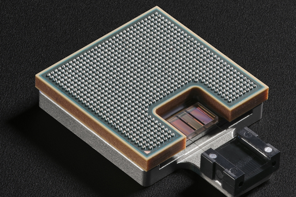
Silicon Box offers design flexibility and exceptional electrical performance at a lower cost and power consumption with its proprietary fabrication method. They have developed the shortest interconnections using sub-5-micron technology, setting a new standard in semiconductor design cycles. This means the industry can efficiently scale chiplet-based solutions across the semiconductor value chain.
Benefits include:
Silicon Box's one-of-a-kind fabrication method increases design flexibility, providing better electrical performance.
• Cost-savings without compromising on power as Silicon Box delivers exceptional results at lower cost and power consumption.
• Benefit from the shortest interconnections, engineered using advanced sub-5-micron technology, ensuring quicker scaling of chiplet-based solutions.
• Leverage the advantages of chiplets that allow larger systems to be built economically with optimised power consumption and higher performance.
• Tap into Silicon Box's partnerships with industry leaders for next-generation chiplet-based solutions, demonstrating their credible expertise and readiness to meet market demands.
The benefits for chip designers result are claimed to be in double computing performance at a fraction of the cost compared to traditional approaches. For graphical processors and high-performance computing chips, costs can be reduced by up to four times. This is a 'new paradigm' in the chip industry, where stakeholders can concentrate on enhancing the performance optimisation of these modular functional units.
ESG and resource efficiency of the factory
• A reverse osmosis de-ionized (RO-DI) water filtration system that purifies NeWater for manufacturing processes
• A fully contained wastewater treatment facility enables 50% of post-manufacturing wastewater to be recycled and reused
• Multi-grid voltage systems and solar panels improve transmission lines' capacity and distribute power consumption more efficiently
• Energy-efficient window glass, blinds, and high-quality insulation reduce the energy required for cooling
Simultaneously, Silicon Box’s integration methods enable high-performance solutions with low power consumption, allowing collaborators to design and build for a more sustainable future. At its core, this cutting-edge offering is not only for manufacturers but retailers and consumers. The ripple effects extend beyond sheer dollars and cents, the predicted economic surge spans multiple sectors due to the interwoven nature of today’s supply chains. This expansion in Asia marks more than widened industrial horizons; it preludes a shift to innovation-led growth brewing within Singapore’s borders.


