Analog Devices invests Oregon expansion

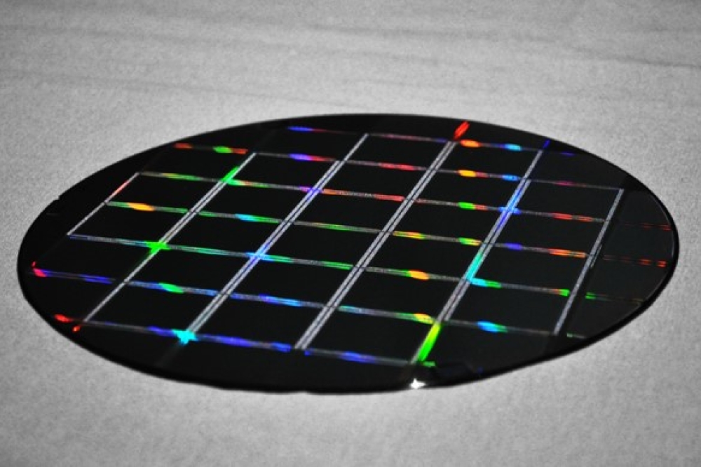
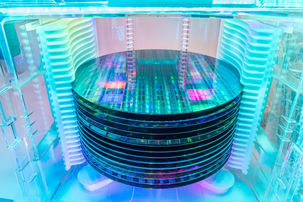
Analog Devices has celebrated its more than $1 billion investment to expand its semiconductor wafer fab in Beaverton, Oregon.
The Beaverton site, built in 1978, is ADI’s largest wafer fabrication facility by volume and serves customers in critical industries, such as industrial, automotive, communications, consumer, and healthcare.
The facility investment expands cleanroom space to about 118,000 sq-ft and nearly doubles internal manufacturing of products running on the 180-nanometer technology node and above. It is also expected to create hundreds of new, long-term employment opportunities, a significant increase to ADI’s current roughly 950 employees in Oregon.
More than 10% of the total investment is for new, state-of-the-art fab tools intended to increase overall efficiency and utilize chemistries that are more environmentally friendly. Despite nearly doubling production output, the facility is targeting to reduce absolute greenhouse gas emissions by approximately 75% and water usage per production unit by approximately 50%.
"By expanding ADI’s Beaverton facility, we are increasing our production capacity in critical industries, boosting domestic manufacturing in line with the vision of the CHIPS Act, and enhancing the global resiliency of ADI’s hybrid manufacturing model," said Vincent Roche, ADI’s CEO and Chair. "While our investment in Beaverton will facilitate these goals, they will be achieved through the incredible dedication and talent of ADI's existing workforce and further tapping into Oregon's strong talent pool."
Commenting on the announcement, U.S. Senator Ron Wyden of Oregon said, “Today’s good news from Analog Devices marks a significant step to ensure Oregon is taking full advantage of the federal CHIPS Act I worked to pass into law. This announcement strengthens a signature industry in Oregon by solidifying semiconductors’ place in the Silicon Forest and beyond, creating statewide impact with new good-paying jobs in Beaverton and rippling out to benefit the entire state economy.”
In addition, the Beaverton facility will host the Semiconductor Advanced Manufacturing University (SAMU), a workforce development training center that will offer eight-week courses to train groups of around 25 students each on semiconductor equipment maintenance. A key driver of ADI’s efforts with the training center is providing training opportunities to many diverse groups within the local community, including U.S. military veterans, people re-entering the workforce, and existing ADI factory operators, to learn semiconductor manufacturing fundamentals and other curriculum to advance their professional development.
ADI’s hybrid manufacturing model is a broad network of internal factories and external partners. This model enables effective management of ADI operations through economic cycles, enhances the resiliency of its global supply chain, and better serves its customer needs. To improve ADI-owned operations, the company has increased capital investment to a high single-digit percent of revenue in fiscal year 2022 and to date in fiscal year 2023 from its historical precedent of around four percent. These manufacturing investments span the globe, including in the states of Washington and Massachusetts, as well as in Ireland, Thailand, Malaysia, and the Philippines.


