TSMC inaugurates Global R&D Center
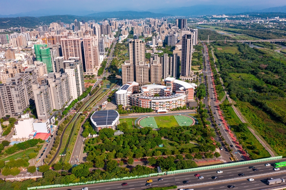
TSMC held an inauguration ceremony for its global Research and Development Center in Hsinchu, Taiwan, celebrating the Company’s newest hub for bringing the next generations of semiconductor technology into reality with customers, R&D partners in industry and academia, design ecosystem partners, and senior government leaders.
The R&D Center will serve as the new home for TSMC’s R&D Organization, including the researchers who will develop TSMC’s leading-edge process technology at the 2-nanometer generation and beyond, as well as scientists and scholars blazing the trail with exploratory research into fields such as novel materials and transistor structures. With R&D employees already relocating to their workplaces in the new building, it will be ready for its full complement of more than 7,000 staff by September 2023.
“The brilliant minds that we will gather together here at our global R&D Center will be working to answer today’s most challenging questions in semiconductor technology, as well as future questions that we have not even imagined,” said TSMC Chairman Dr. Mark Liu. “I am eagerly looking forward to seeing the solutions and technologies that will emerge from here in the decades to come.”
TSMC Founder Dr. Morris Chang, Chairman Dr. Mark Liu, and CEO Dr. CC Wei presided over the inauguration ceremony, which brought together honored guests from customers, R&D partners, universities, design ecosystem partners, industry associations, and senior government officials including Premier Chen Chien-Jen, National Science and Technology Council Minister Wu Tsung-Tsong, Minister of Economic Affairs Wang Mei-Hua, and Hsinchu County Magistrate Yang Wen-Ke. In total, more than 200 attendees joined the event.
“As we celebrate this milestone for TSMC R&D, I would like to thank our customers for their trust in us to deliver the right technology at the right time for them,” said TSMC CEO Dr. C.C. Wei. “I would also like to thank our R&D team for making that possible. Your tireless curiosity and courage in accepting challenges enables TSMC to drive technology forward and help customers bring groundbreaking innovations to life.”
TSMC’s R&D Center has total floor space of 300,000 square meters, or approximately 42 standard soccer fields. It is designed as a green building with features such as vegetated walls, rainwater collection tanks, and windows that maximize natural light, as well as rooftop solar panels capable of generating 287 kilowatts at peak conditions, demonstrating TSMC’s commitment to sustainability.

