Industry’s fastest, highest-capacity HBM?

First in industry to launch 8-high 24GB HBM3 Gen2 with bandwidth over 1.2TB/s and 'superior power efficiency' enabled by advanced 1β process node.
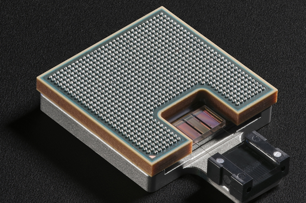
Micron Technology has begun sampling what it says is the industry’s first 8-high 24GB HBM3 Gen2 memory with bandwidth greater than 1.2TB/s and pin speed over 9.2Gb/s, which is up to a 50% improvement over currently shipping HBM3 solutions. With a 2.5 times performance per watt improvement over previous generations, Micron’s HBM3 Gen2 offering is claimed to set new records for the critical artificial intelligence (AI) data center metrics of performance, capacity and power efficiency. These Micron improvements reduce training times of large language models like GPT-4 and beyond, deliver efficient infrastructure use for AI inference and provide superior total cost of ownership (TCO).
The foundation of Micron’s high-bandwidth memory (HBM) solution is Micron’s 1β (1-beta) DRAM process node, which allows a 24Gb DRAM die to be assembled into an 8-high cube within an industry-standard package dimension. Moreover, Micron’s 12-high stack with 36GB capacity will begin sampling in the first quarter of calendar 2024. Micron says that it provides 50% more capacity for a given stack height compared to existing competitive solutions. Micron’s HBM3 Gen2 performance-to-power ratio and pin speed improvements are critical for managing the extreme power demands of today’s AI data centers. The improved power efficiency is possible because of Micron advancements such as doubling of the through-silicon vias (TSVs) over competitive HBM3 offerings, thermal impedance reduction through a five-time increase in metal density, and an energy-efficient data path design.
Micron is proud to be a partner in TSMC’s 3DFabric Alliance and to help shape the future of semiconductor and system innovations. As part of the HBM3 Gen2 product development effort, the collaboration between Micron and TSMC lays the foundation for a smooth introduction and integration in compute systems for AI and HPC design applications. TSMC has received samples of Micron’s HBM3 Gen2 memory and is working closely with Micron for further evaluation and tests that will benefit customers’ innovation for the next-generation HPC application.
The Micron HBM3 Gen2 solution addresses increasing demands in the world of generative AI for multimodal, multitrillion-parameter AI models. With 24GB of capacity per cube and more than 9.2Gb/s of pin speed, the training time for large language models is reduced by more than 30% and results in lower TCO. Additionally, the Micron offering unlocks a significant increase in queries per day, enabling trained models to be used more efficiently. Micron HBM3 Gen2 memory’s best-in-class performance per watt drives tangible cost savings for modern AI data centers. For an installation of 10 million GPUs, every five watts of power savings per HBM cube is estimated to save operational expenses of up to $550 million over five years.
“Micron’s HBM3 Gen2 technology was developed with a focus on unleashing superior AI and high-performance computing solutions for our customers and the industry,” said Praveen Vaidyanathan, vice president and general manager of Micron’s Compute Products Group. “One important criterion for us has been the ease of integrating our HBM3 Gen2 product into our customers’ platforms. A fully programmable Memory Built-In Self Test (MBIST) that can run at the full specification pin speed positions us for improved testing capability with our customers, creates more efficient collaboration and delivers a faster time to market.”
“At the core of generative AI is accelerated computing, which benefits from HBM high bandwidth with energy efficiency,” said Ian Buck, vice president of Hyperscale and HPC Computing at NVIDIA. “We have a long history of collaborating with Micron across a wide range of products and are eager to be working with them on HBM3 Gen2 to supercharge AI innovation.”
Micron developed this breakthrough product by leveraging its global engineering organization, with design and process development in the United States, memory fabrication in Japan and advanced packaging in Taiwan. Micron previously announced its 1α (1-alpha) 24Gb monolithic DRAM die-based 96GB DDR5 modules for capacity-hungry server solutions and has now introduced the1β 24Gb die-based 24GB HBM3 offering. In the first half of calendar 2024, the company plans to make available its 1β 32Gb monolithic DRAM die-based 128GB DDR5 modules. These offerings demonstrate Micron’s technology innovations for AI servers.


