Brewer Science to unveil innovative advanced packaging solutions

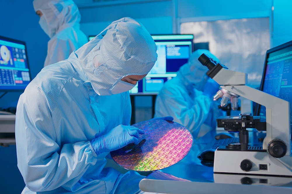
Brewer Science will present new developments in temporary and permanent bonding material technologies for advanced packaging at Asia’s two premier technology conferences, Advanced Packaging Summit on September 5th and SEMICON Taiwan from September 6th – 8th.
Dr. Dongshun Bai, Brewer Science's Senior Technologist & Business Development Director, spearheads a decade-spanning journey in semiconductor advancements. His expertise will be on display at the Advanced Packaging Summit, hosted by SEMI, where he will delve into his presentation titled "Novel Materials for Advanced Packaging". Dr. Bai will discuss new material improvements for advanced packaging, focusing on excellent bonding uniformity, optimizing adhesion for high-density substrates, ensuring high-temperature stability, and groundbreaking innovations in surface modification.
Brewer Science continues at SEMICON Taiwan, hosted at the TaiNEX 1&2 in Taipei from September 6th to 8th. Ms. Rama Puligadda, Chief Technical Officer at Brewer Science, takes the stage at the Heterogeneous Integration Global Summit. Scheduled for September 7th at 11:50am (Taipei Time), her presentation, "Recent Advances in Materials for Advanced Packaging", will illuminate advancements powering hybrid bonding, fan-out packaging, 3D/2.5D technology, and embedded solutions for heterogeneous semiconductor integration.
Ms. Puligadda's presentation will underscore the pivotal role of materials innovation in enabling cutting-edge packaging technologies. Addressing challenges in 3D/2.5D packaging, flexible solutions, and fan-out packaging, her insights will unveil how Brewer Science's advanced materials enable innovative packaging design, miniaturization, functionality, and cost-effectiveness.
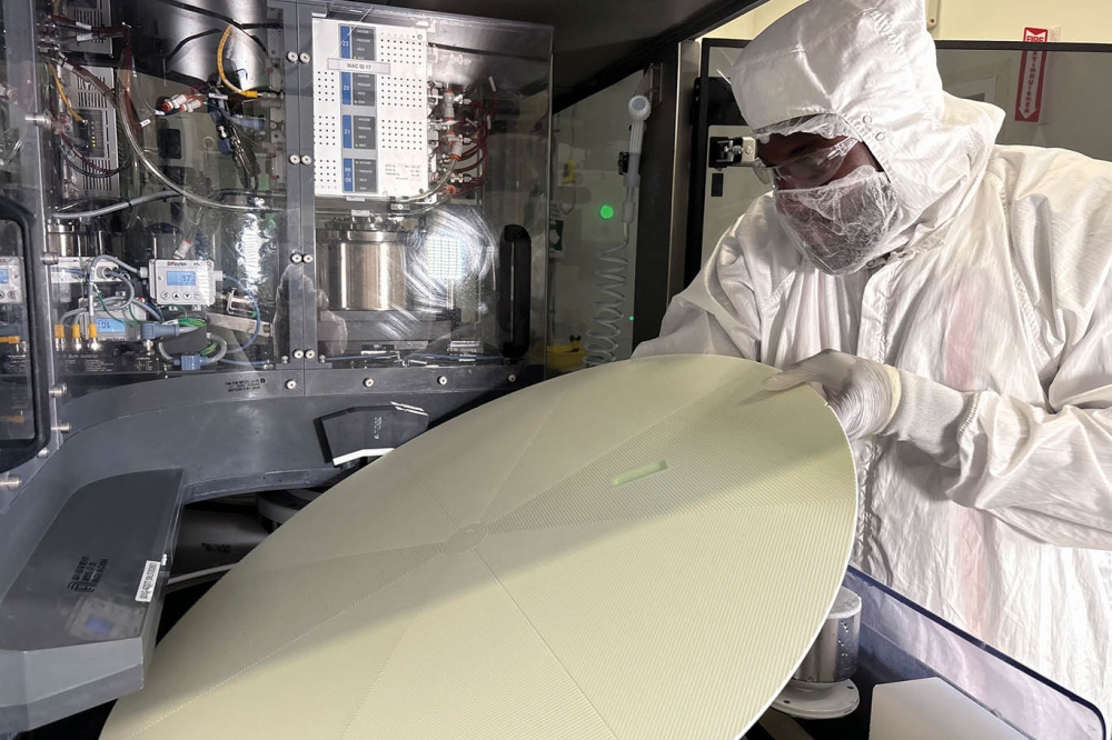
In conjunction with the events, Brewer Science announces the launch of BrewerBOND® 703 laser release material, which reduces the risk of UV damage during laser debonding. The new material combines high UV absorption capabilities with ultra-low UV transmittance properties to provide a safeguard against UV laser energy interference on delicate device wafers. Learn more about this material by visiting Brewer Science's booth at SEMICON Taiwan or submitting an inquiry through the company's official website.
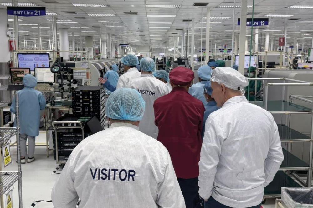
Throughout the events, Brewer Science's experts will be stationed at booth K2470 in the SEMICON Taiwan Exhibit Hall, available for engaging discussions and insightful demonstrations. Join them on:
• Wednesday, September 6: 10:00am–5:00pm
• Thursday, September 7: 10:00am–5:00pm
• Friday, September 8: 10:00am–4:00pm
For those unable to attend the conferences, Brewer Science extends an open invitation to explore their Temporary Bonding and Debonding Services and Permanent Bonding Materials webpages. You can also request datasheets or schedule expert-led consultations through the company's website.