
EV Group at SEMICON Taiwan
Papers to highlight breakthrough capabilities of EVG’s hybrid bonding and metrology solutions for heterogeneous integration, and NIL solutions for meta-optics and AR waveguide manufacturing.
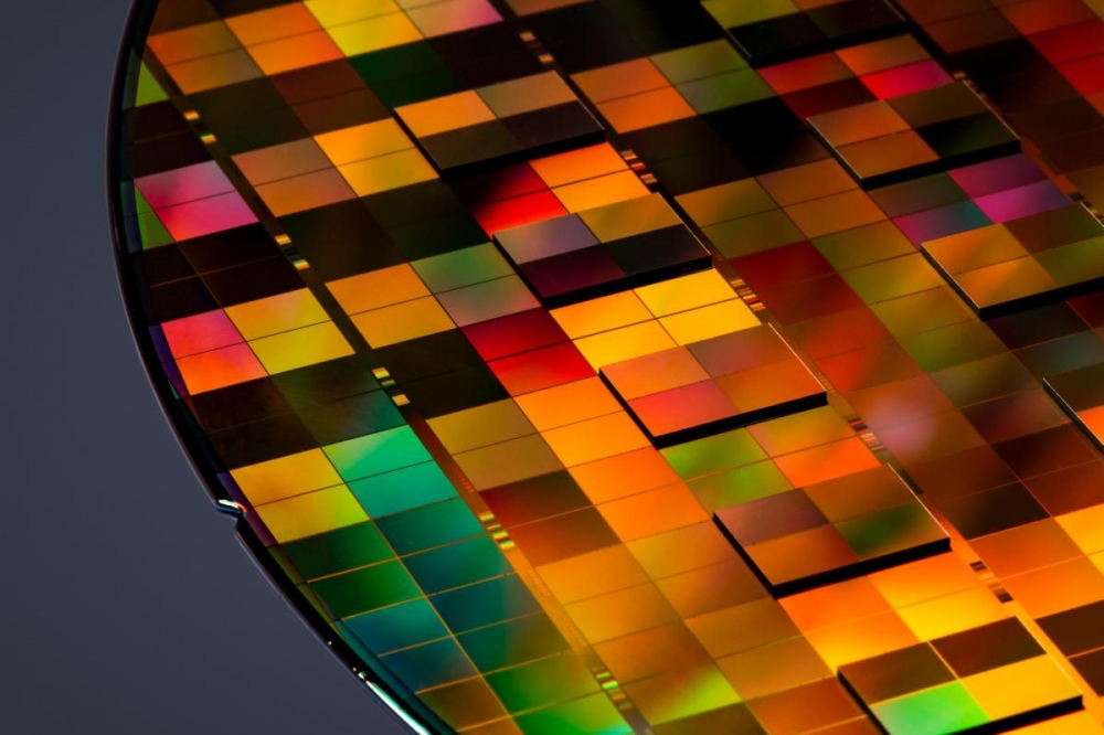
EV Group (EVG), a leading supplier of wafer bonding and lithography equipment for the MEMS, nanotechnology and semiconductor markets, has announced that new developments in 3D/heterogeneous integration and augmented reality (AR) waveguide manufacturing enabled by its advanced wafer-to-wafer (W2W) and die-to-wafer (D2W) hybrid bonding, metrology, and nanoimprint lithography (NIL) solutions will be highlighted at the SEMICON Taiwan 2023 expo in Taipei, Taiwan. At SEMICON Taiwan, EVG will present the following papers:
* “Exploring the Synergy of Nanoimprint Lithography, Meta Lenses, and AR/VR” (MEMS and Sensors Forum – Tue., September 5, 2:00pm at Room 505ab, 5th Floor, TaiNEX 1)
Thomas Uhrmann, director of business development at EVG, presents an overview of the versatility and recent achievements of NIL, with a focus on meta lenses and AR waveguide manufacturing, and how the capabilities of this technology are rapidly emerging. He will discuss how in order to achieve efficient scaling of these precise structures, it is necessary to match mastering techniques, proven replication processes, and dedicated optical materials.
* “Advances in Metrology for 3D and Heterogeneous Integration” (TechXPOT – Wed., September 6, 2:00pm at Booth L1100, 4th Floor, TaiNEX 1)
Jason Li, process engineer in the Technology Development & IP department at EVG Taiwan, will provide an overview of the current overlay metrology requirements for various applications, including D2W, W2W, and die shift in novel packaging methods, such as maskless lithography with adaptive patterning. Understanding and addressing these metrology needs are crucial for advancing 3D and heterogeneous integration technologies, and achieving efficient and reliable production yields.
* “Next Generation Logic and Memory Manufacturing by Wafer-to-Wafer Bonding: A Holistic View” (IC Forum – Fri., September 8, 2:00pm at Room 402, 4th Floor, TaiNEX 1)
Paul Lindner, executive technology director and member of the executive board at EVG, will provide an overview of current industry trends concerning next-generation memory and logic devices, focusing on how 3D integration enables new technological advancements. This will include discussion of the combination of fusion and hybrid bonding, as well as ultra-thin layer splitting techniques, which represent the new lithography scaling for advanced semiconductor devices.
* “Breaking Boundaries: Exploring Hybrid Chip-to-Wafer and Wafer-to-Wafer Bonding for 3D-IC Integration” (Heterogeneous Integration Global Summit – Fri., September 8, 2:40pm at Room 401, 4th Floor, TaiNEX 1)
Thomas Uhrmann will provide an overview of the current industry trends and technological advancements in W2W and D2W hybrid bonding, including key technology differentiators and integration scenarios. The next technological transformation will introduce a universal high-density interconnect technology, thus instigating a new integration process. The choice of integration flow will depend on factors such as interconnect density, chip size, system yield, and cost.
EVG’s wafer bonding, lithography and metrology solutions enable the development and high-volume manufacturing of technology innovations in advanced packaging—including backside illuminated CMOS image sensors and other 3D-IC stacked devices—as well as in MEMS and compound semiconductors. Recent breakthroughs in hybrid bonding to address the needs for 3D device integration, wafer bond alignment technology to address future 3D-IC packaging requirements, IR laser release technology to eliminate glass substrates for advanced packaging and enable thin-layer 3D stacking, maskless exposure for fan-out wafer level packaging (FOWLP), and NIL to support wafer-level optics (WLO) manufacturing, are just a few examples of EVG’s technology leadership in heterogeneous integration and wafer-level packaging.
EVG also engages with companies and research groups across the technology supply chain to develop high-volume manufacturing solutions that drive new innovations in semiconductors, sensors and photonics for a wide variety of automotive, medical, industrial and home entertainment applications.


