Loading...
News Article

Mitsubishi Electric completes Fukuyama installation

News

Aims to help realize a carbon-free society through the stable supply of power semiconductor devices.

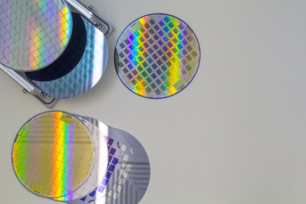
Mitsubishi Electric Chas completed installation of its first 12-inch silicon wafer processing line at its Power Device Work’s Fukuyama Factory, which manufactures power semiconductors. In addition, through sample production and testing, it has been verified that the power semiconductor chips processed on this production line achieve the required performance levels.

As previously announced, Mitsubishi Electric is planning to start mass production on the new 12-inch silicon wafer line in fiscal 2025. The company aims to approximately double its silicon power semiconductor wafer processing capacity by fiscal 2026 compared to fiscal 2021 levels.

In recent years, the demand for power semiconductors offering efficient control of electrical power is growing as countries look to achieve carbon-free status. Power semiconductors are utilized in wide range of relevant products, including electric vehicles, consumer devices (e.g. air-conditioning systems), industrial equipment, renewable energy and traction devices, and a stable supply is required in order to meet this growing demand.

Mitsubishi Electric will contribute to the realization of a carbon-free society through enhancement of its production capacity and by ensuring a stable supply of power semiconductors through the introduction of highly efficient 12-inch wafer production lines.

Silicon photonics: accelerating growth in the race for high-speed optical interconnects
CCD-in-CMOS technology enables ultra-fast burst mode imaging
2025 6G A look forward
Critical Manufacturing climbs Deloitte’s Technology Fast 50
Semiconductors: The most important thing you probably know the least about
Imec and partners unveil SWIR sensor with lead-free quantum dot photodiodes
Lattice introduces small and mid-range FPGA offerings
SEMI and SMT inspection solutions at NEPCON Japan 2025
Nordic Semiconductor and Kigen demonstrate Remote SIM Provisioning for Massive IoT
Spirent collaborates with Siemens
Quobly forges strategic collaboration with STMicroelectronics
New standards in pressure measurement systems for the semiconductor industry
IBM delivers optics breakthrough
Semiconductor equipment sales to reach $139 Billion in 2026
Marvell introduces 1.6 Tbps LPO Chipset
ACM research strengthens Atomic Layer Deposition portfolio
CEA-Leti demonstrates embedded FeRAM platform compatible with 22nm FD-SOI node
Lattice introduces small and mid-range FPGA offerings
Solace unlocks full potential of event-driven integration
Advantest to showcase latest test solutions at SEMICON Japan 2024
CEA-Leti device integrates light sensing and modulation
Nordic launches Thingy:91 X prototyping platform for cellular IoT and Wi-Fi locationing
Imec achieves seamless InP Chiplet integration on 300mm RF Silicon Interposer
High-precision SMU
Powering India’s energy future
China’s Nvidia probe puts global investors ‘on notice’
POET Technologies appoints new director
Imec demonstrates core building blocks of a scalable, CMOS-fab compatible superconducting digital technology
Imec proposes double-row CFET for the A7 technology node
ULVAC launches new deposition system
Beebolt and SEMI Announce Strategic Partnership to Drive Supplier Resilience and Agility
esmo group introduces Automated Final Test Manipulator
×
Search the news archive

To close this popup you can press escape or click the close icon.
Logo
x
Logo
×
Register - Step 1

You may choose to subscribe to the Silicon Semiconductor Magazine, the Silicon Semiconductor Newsletter, or both. You may also request additional information if required, before submitting your application.


Please subscribe me to:


You chose the industry type of "Other"

Please enter the industry that you work in: