
Advanced SAM validates integrity of electrostatic chucks
Scanning Acoustic Microscopy provides 'superior' inspection of sintered electrostatic chucks used to handle wafers in semiconductor fabrication by detecting minuscule defects within multiple layers of material.
The semiconductor fabrication industry now has an advanced new quality inspection tool called Scanning Acoustic Microscopy at its disposal that can dramatically improve the reliability of the electrostatic chucks used to hold wafers during processes such as vapor deposition and etching.
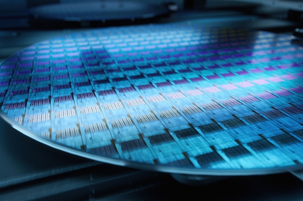
Electrostatic chucks (ESCs) utilize a platen with embedded electrodes that are energized with high voltage to establish an electrostatic holding force that can be used to “grip” very delicate items such as wafers, foils, or films. ESCs are built in layers, with a layer of screen-printed electrodes sandwiched between layers of insulative ceramic material. The entire structure is then sintered to create a single chuck.
With ESCs so integral to the wafer production process, one challenge has been the lack of high-resolution tools capable of inspecting multiple layers of sintered material to validate the integrity of the package. ESCs made in this manner can display fluctuations or non-uniformities in the thickness of the dielectric layer as well as extremely small cracks and pores that can adversely affect the chuck’s ability to electrostatically secure items.
Since ESCs must be constructed and perform flawlessly to maintain the extreme precision required in semiconductor wafer production, Scanning Acoustic Microscopy (SAM) has become an important new tool for the industry to validate ESC integrity during manufacture.
SAM is a non-invasive, non-destructive ultrasonic testing method. The testing is already the industry standard for 100% inspection of semiconductor components to identify defects such as voids, cracks, and the delamination of different layers within microelectronic devices. Now, the same rigor of quality testing and failure analysis is being applied to ensure ESC integrity.
“SAM can not only detect fluctuations in the thickness of the dielectric layer but also the presence of extremely small cracks and pores which could compromise the ESC’s ability to electrostatically secure the substrate to the chucking surface. It is essentially the equivalent of an x-ray inside the part, so is a comprehensive test method to ensure quality,” says Hari Polu, President of OKOS, a Virginia-based manufacturer of SAM and industrial ultrasonic non-destructive (NDT) systems. OKOS is a wholly owned subsidiary of PVA TePla AG, Germany and offers both manual and automated inspection systems for flat panels, thin plates, circular discs, sputtering targets, and special alloys.
The Many Benefits of SAM for ESC Inspection
For validating the integrity of electrostatic chucks, advanced, phased array Scanning Acoustic Microscopy works by directing focused sound from a transducer at a small point on a target object. The sound hitting the object is either scattered, absorbed, reflected, or transmitted. By detecting the direction of scattered pulses as well as the “time of flight,” the presence of a boundary or object can be determined as well as its distance.
To produce an image, samples are scanned point by point and line by line. Scanning modes range from single layer views to tray scans and cross-sections. Multi-layer scans can include up to 50 independent layers. Depth-specific information can be extracted and applied to create two- and three-dimensional images without the need for time-consuming tomographic scan procedures and more costly x-rays. The images are then analyzed to detect and characterize flaws such as any irregularities in the thickness of the ESC’s dielectric layer as well as miniscule cracks and pores.
“OKOS has leveraged the lessons and the tight specifications from the semiconductor world and adapted our SAM scanning systems to provide unique solutions specifically for electrostatic chuck quality inspection, said Polu. “With this type of testing, we can inspect materials at a level one to two orders of magnitude better than traditional options to discover defects such as voids, cracks, and the delamination of different layers as small as 50-microns that were previously undetected.”
Companies like OKOS offer a range of SAM products from compact, tabletop units to fully automated production line systems.
When high throughput is required for 100% inspection, ultra-fast single or dual gantry scanning systems are utilized along with 128 sensors for phased array scanning. Multiple transducers can also be used to simultaneously scan for higher throughput.
As important as the physical and mechanical aspects of conducting a scan, the software is critical to improving the resolution and analyzing the information to produce detailed scans. Multi-axis scan options enable A, B, and C-scans, contour following, off-line analysis, and virtual rescanning for ESCs, which result in highly accurate internal and external inspection for defects via the inspection software.
Various software modes can be simple and user friendly, advanced for detailed analysis, or automated for production scanning. An off-line analysis mode is also available for virtual scanning.
“OKOS decided early on to deliver a software-driven, ecosystem-based solution,” said Polu. The company’s ODIS Acoustic Microscopy software supports a wide range of transducer frequencies from 2.25 to 230 MHz.
Polu estimates that the software-driven model enables them to drive down the costs of SAM testing while delivering the same quality of inspection results. As a result, this type of equipment is well within reach of even modest testing labs, R&D centers, and material research groups.
“Every semiconductor fabricator will eventually move towards this level of inspection for ESC quality control because the level of detection is far superior to conventional methods. The increased accuracy, reliability, and comprehensiveness as well as decreased cost and time involved are driving the change.” concludes Polu.
When fabricators take advantage of the higher level of failure detection and analysis, the production yield and overall reliability of wafers and semiconductors improve significantly, and potential points of failure are eliminated.


