Advanced packaging market nears US$90 billion

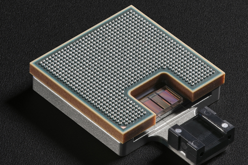
Various packaging technologies, including 2.5D and 3D packaging, fan-out wafer-level packaging (FOWLP), system-in-package (SiP), flip-chip packaging, wafer-level chip-scale packaging (WLCSP) will contribute heavily to the dynamic landscape of advanced semiconductor packaging.
Predominantly driven by climbing sales of consumer electronics, and faster penetration of emerging technologies, the market for advanced semiconductor packaging is poised for remarkable growth in the years to come, according to a recent report from Fairfield Market Research. At a projected CAGR of approximately 10.8% between 2023 and 2030, the market growth trajectory is expected to proliferate through the end of forecast period, reaching in excess of US$90 Bn by the end of this decade.
The advanced semiconductor packaging market revolves around the development, integration, and enhancement of packaging technologies for semiconductor devices. Integrated circuits (ICs) or chips, being the core of electronic devices, require safeguarding, connectivity, and support. Advanced semiconductor packaging provides the necessary mechanical stability, thermal management, and electrical connections to ICs.
Technological advancements in semiconductors will be the strongest driving force for market, says the recently published report of Fairfield Market Research, on the global advanced semiconductor packaging industry.
The rising complexity of ICs has led to higher wafer production costs, which bolsters the demand for advanced semiconductor packaging is being adopted to optimise the integration of processors, memory, and accelerators for AI and machine learning applications.
“While the market has been on a robust growth trajectory, partly due to increased demand from the investment community, it is the shifting consumer preferences and a constant innovation drive in consumer electronics that will be instrumental in robust market growth in the upcoming years,” remarks the company analyst.
Key Research Insights
• Fan-out wafer-level packaging (FOWLP) continues to dominate the advanced semiconductor packaging market.
• The consumer electronics sector held the largest share of revenue in the advanced semiconductor packaging market in 2022.
• Asia Pacific is expected to remain the global leader while North America gears up for the fastest CAGR through 2030.
FOWLP Type Prominent
The report attributes the dominance of FOWLP in the advanced semiconductor packaging market to its sustained popularity in consumer electronics, advances in heterogeneous integration, and improved performance and stability.
The FOWLP type of packaging finds wide application in mobile devices like smartphones, tablets, and smartwatches, offering a solution for creating compact yet high-performing devices. By integrating multiple chips such as application processors, memory, and power management units into a single package, FOWLP further enhances the functionality and performance of electronic devices.
FOWLP's small form factor, high interconnect density, and excellent electrical performance make it an ideal platform for packaging MEMS and sensors. This technology enables the integration of MEMS components, sensor chips, and signal conditioning circuitry, resulting in compact yet highly effective sensor modules.
Consumer Electronics Industry Top Demand Generator
The consumer electronics sector is expected to drive demand swiftly during the forecast period. Advanced packaging is vital for producing smaller, more powerful, and feature-rich consumer electronics. High-resolution display technologies such as OLED, and micro-LED screens particularly benefit from advanced semiconductor packaging.
Innovative packaging techniques like flip-chip packaging and chip-on-glass (COG) ensure high-speed data transfer and efficient power distribution, enabling thin, flexible displays with excellent contrast ratios and low power consumption.
In the realm of smart TVs, advanced semiconductor packaging plays a critical role in enabling features such as networking, multimedia processing, and high-resolution screens.
Key Report Highlights
• Integration of components like application processors, graphics chips, memory, and more enhanced performance, power efficiency, and capabilities like video streaming and voice control will also boost the expansion of the advanced semiconductor packaging market space.
• Packaging technologies like flip-chip packaging, chip-on-glass (COG), and system-in-package (SiP) are enabling the integration of sensors, processors, and memory in ADAS systems, in turn enhancing vehicle intelligence and safety.
Insights into Regional Analysis
Asia Pacific Leads the Regional Ranking Board
The Asia Pacific region will maintain its lead in the advanced semiconductor packaging market, which is majorly driven by the booming semiconductor industry.
Countries such as China, South Korea, Taiwan, and Japan are at the forefront and this trend will prevail throughout the period of assessment. These countries are thus likely to be setting the stage for cutting-edge packaging solutions in the years to come.
The region's increasing demand for innovative packaging technologies is propelled by the rapid developments and expansion of automotive, and consumer electronics industries, as well as the rise of emerging technologies like 5G, AI, and IoT.
Japan’s growing focus on ADAS, and autonomous driving technologies will create a solid stream of opportunities, says the report. The semiconductor packaging plays a crucial role here for its higher durability, temperature control, and high-performance interconnects.
North America Set for Rapid Growth Through 2030
North America is all geared up for rapid growth in the global advanced semiconductor packaging market. The region is at the forefront of AI and ML technology, emphasizing cutting-edge hardware development. Pacing EV adoption, and the widening scope for sustainable transportation solutions in the US further fuel the demand for advanced packaging technologies.
The US market is especially awaiting substantial growth as it caters to the increasing demand for high-reliability, efficient thermal management, and small form factor packaging solutions in the EV and sustainable transportation sectors.


