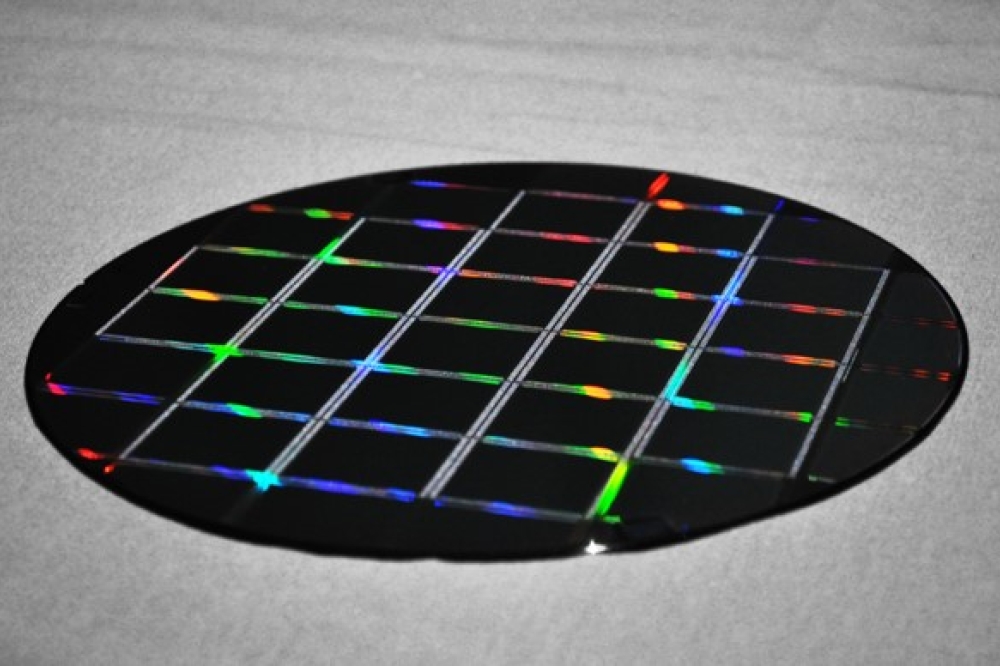
Wafer cleaning market to reach US$ 17.2 billion
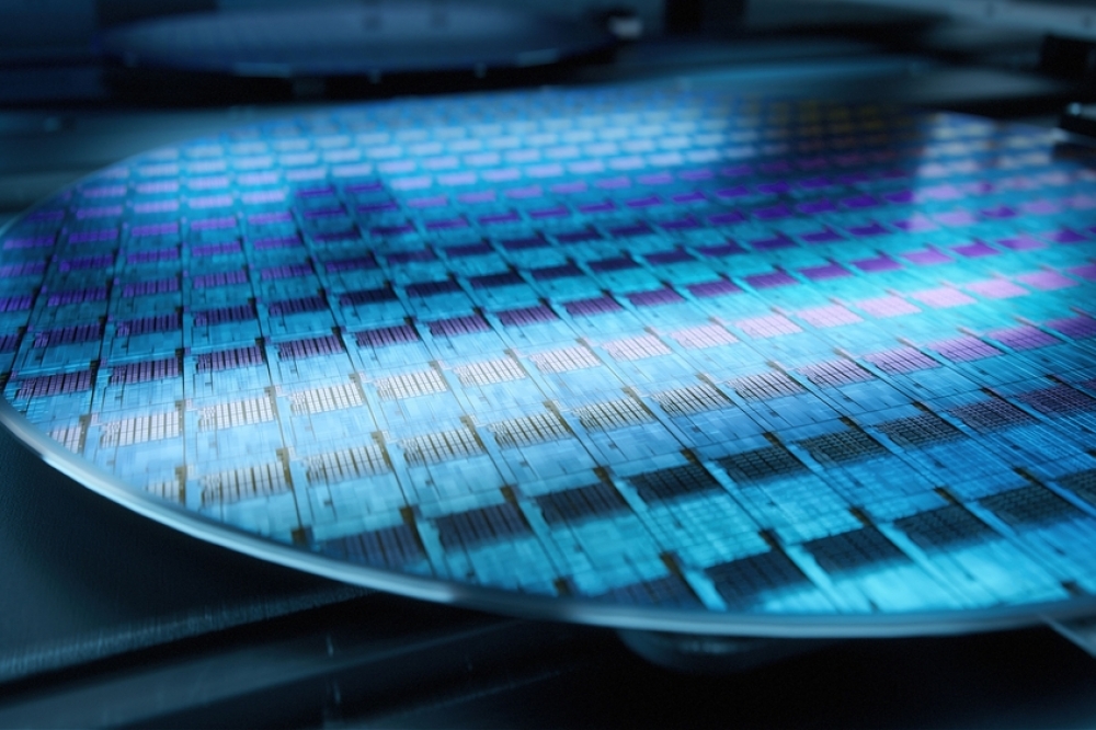
According to a Future Market Insights (FMI) report, the wafer cleaning equipment market is projected to reach US$ 8.3 Billion by 2023 and US$ 17.2 Billion by 2033 growing at a CAGR of 7.5%.
With the rapid growth of the semiconductor industry and increasing consumer electronics demand, wafer-cleaning equipment is on the rise.
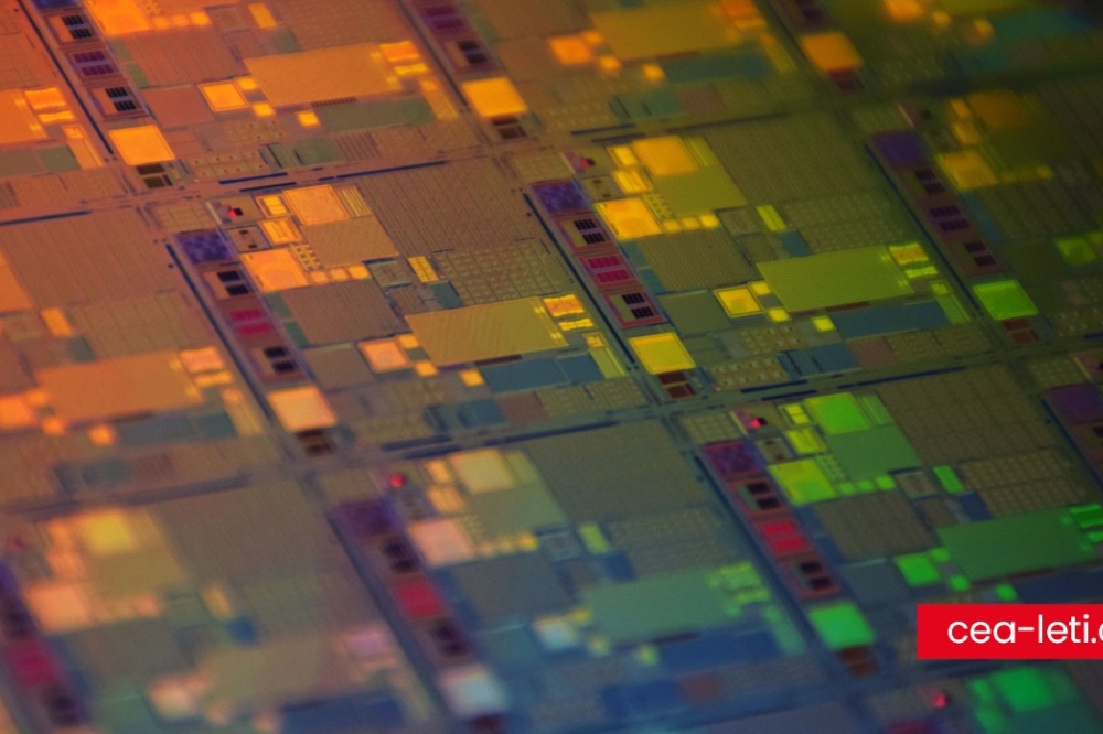
Equipment designed for wafer cleaning removes particles, residues, and contaminants. As a result, semiconductor devices that are fabricated on the wafer have higher yields and better quality than those fabricated on plain wafers. Technology advancements and expansion of the semiconductor industry drive demand for wafer cleaning equipment. With the development of more advanced semiconductor devices, the need for cleaner wafers is becoming more prevalent.
With the progress of semiconductor technology, wafer cleaning requirements are becoming increasingly stringent. Due to the increasing size and complexity of features, new cleaning methods and equipment are expected to grow in demand in growing years. Increasing semiconductor production capacity can increase the demand for wafer-cleaning equipment as new semiconductor fabrication facilities are built or expanded.
There is a continuous need for more powerful and smaller semiconductor components as consumer electronics, automotive electronics, IoT devices, and other advanced technologies continue to progress. With growing production capacity, wafer-cleaning equipment can be in higher demand as semiconductor companies increase their research and development activities. The economy of a particular region or country improves, and the semiconductor market will likely grow in demand, which consequently will increase the demand for wafer-cleaning machines. Environmental sustainability and regulations regarding the use of certain cleaning chemicals could influence a shift toward eco-friendly and efficient cleaning products.
Key Takeaways:
· Batch spray cleaning systems are expected to grow at a 4% CAGR between 2023 and 2033.
· Wafer cleaning equipment innovation demand in Japan is expected to grow at a CAGR of 9% by 2033, according to industry analysts.
· The United States wafer cleaning equipment market is expected to grow at a 6.4% CAGR by 2033.
· The South Korean market for wafer cleaning equipment is expected to reach US$ 693.9 Million by 2033.
· According to industry forecasts, LED applications will experience a CAGR of 3% over the next few years.
“The rising popularity of semiconductors in consumer electronics and the need for cost-effective products will fuel demand. With the rise of aerospace and defense industries, and increased investment in research and development activities, the market is expected to grow," says an FMI analyst.
Competitive Landscape:
The wafer-cleaning equipment market features a wide range of products from numerous key players. These companies' competition is influenced by numerous factors, including innovative products, reasonable prices, and environmentally friendly options.
As a way to keep up with changing customer needs, introduce new designs, and enhance performance, they invest heavily in research and development. The expansion of a company's market presence is often accomplished through partnerships, mergers, and acquisitions.
Market Developments Include:
· In February 2023, Amtech Systems, Inc. introduced the 20th double-sided OnTrak wafer scrubber system for SiC manufacturing applications. With configurations of 100-200mm wafers and custom-designed carriers to accommodate even smaller wafers, the new OnTrak double-sided scrubber is ideally suited to compound semiconductor applications.
· In May 2023, Zhejiang Sineva Intelligent Technology Co, a technology company specializing in mobile robotic solutions and focusing on improving the efficiency of plants and modernizing them with its global partners, announced the launch of mobile robots. The robots designed to grasp, connect, and handle silicon wafers with accuracy provide an automated loading and unloading system, the company noted, pointing out that the sink robot, which is designed for semiconductor production, mainly cleans wafers and handles tanks.


