
Advanced X-ray technology for advanced packaging
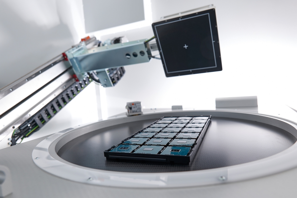
While X-ray technology in the semiconductor industry was considered too inaccurate, too slow, and too expensive a short time ago, new developments in micro-CT, sophisticated trajectories, and smart algorithms are delivering a non-destructive inspection method that is helping manufacturers with their zero-defect strategy taking their productivity and profitability to a new level.
Back in 2005 in an interview marking the 40th anniversary of ‘Moore’s Law’, Moore noted that this miniaturization would soon reach its limits and would probably become physically unfeasible or simply too expensive sometime in the mid-2020s: “...the fact that materials are made of atoms is the fundamental limitation, and it’s not far off...We’re hitting some pretty fundamental limits, so one day we’re going to have to stop making things smaller.” Meanwhile, having arrived in the 2020s, we still haven’t reached the end of the line.
Today, Advanced Packaging has long since moved into the nanometer range regarding electronical structures. Compared to an average human hair of 0.06 mm, i.e., 60,000 nm in diameter, think of microchips sizes of a few square millimeters and their transistors inside acting as miniature electrical switches to turn the electricity on and off. Nowadays, there are several billion transistors per chip!

3D-view of 60 µm micro-bumps, soldered and open
Increasing amounts of dies inside of individual packages are connected in enormous networks of metal traces. Further sub-components inside fine-tuned electrical circuits are bridged via thousands of solder joints with diameter sizes between 5 to 100 µm. These solder joints (balls, C4- or micro-bumps) as well as the TSVs (Through-Silicon Vias) are risks to the product quality, generally caused by production process variations.
The more compact and powerful today’s ICs become and the more complex their production is, the more increases their value - from one production step to the next. Every defective microchip that needs to get sorted out means high financial losses. Imagine the economic damage through a whole series of entirely packaged ICs that are unusable due to a process error not discovered at an early stage! Manufacturers in the semiconductor industry need to aim for zero-defect production defining strict tolerances. And therefore, reliable quality inspections already start in research and development and accompany the entire manufacturing process to reduce the costs of non-quality production processes.

Typical defects of solder joints.
Destructive testing methods, however precise and detailed they may be, can no longer be the solution, given the long turnaround time and high costs involved. Optical inspections on the other edge of the possible inspection technologies only detect a fraction of the critical defects. X-ray technology has received little attention as an inspection method in the semiconductor field. Although it is the only technology which can look inside a product, simple fluoroscopy cannot distinguish the overlapping layers in today’s complex three-dimensional packages. Three-dimensional computed tomography (CT), which images the spatial view of an object, was long considered too slow and too cost-intensive.
Three-dimensional computed laminography (CL) has now changed the game. Unlike CT, CL does not require 360° rotation of the test part. In a special way, the component gets scanned layer by layer, achieving the required resolution and image quality to inspect the critical interconnections. Layers can get analyzed individually or reconstructed into a 3D volume. The 3D volume, in turn, can be cut at any region of interest and examined in detail. In doing so, computed laminography is much faster than, for example, FIB-SEM (Focused Ion Beam Scanning Electron Microscopy) and detailed enough to detect all critical defects. Today’s CT/CL inspection systems ensure consistent image quality and stable, repeatable results even after hours of operation during batch inspection.
In addition, X-ray inspection in the semiconductor industry is becoming even more efficient by applying automated inspection processes and automatic defect recognition (ADR). Comet Yxlon’s high-resolution microfocus X-ray systems, with their best-in-class imaging and latest software features, combined with Dragonfly’s sophisticated deep-learning models for automatic segmentation and image evaluation, can be tailored to individual user requirements and work independently from human bias. Ramp-up processes are accelerated, resulting in significantly shorter time-to-market.

3D-view of voids in solder bumps.
But wait, can’t X-rays damage, or even destroy your sensitive products? That’s no longer the case with the innovative Comet Yxlon inspection systems. Low-dose detector modes for sensitive components, dose monitoring with alarm and stop function, and additional dose reduction kits prevent possible damages through radiation and guarantee safe X-ray inspections. In addition to the proven Cheetah EVO, Cougar EVO, and FF20 CT microfocus systems, Comet Yxlon also offers the FF35 CT as a SEMI version, certified according to the high SEMI® standards, including the hazard and safety standards SEMI® S2-0818 & SEMI® S8-0218. And the developments continue at full steam.


