
SandBox Semiconductor adds hybrid metrology capabilities
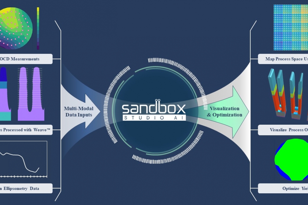
SandBox Studio AI strengthens platform with new product, Weave, to accelerate metrology analysis, reduce development costs, and speed up innovation in advanced chips.
SandBox Semiconductor has launched a new product for its process development platform, SandBox Studio AI.
One of the biggest challenges in the semiconductor industry is developing manufacturing processes for increasingly advanced chip designs with high yield and reliability. Fabrication processes typically involve over a thousand steps that each must be carefully controlled and optimized. Today, this optimization is largely performed by iterative trial and error and requires companies to invest heavily in process development and recipe scaling to meet increasingly stringent manufacturing requirements. As chip technology advances, the complexity of the fabrication process continues to increase.
“SandBox Semiconductor was founded to help process engineers leverage powerful computational models in their day-to-day process development,” said Dr. Meghali Chopra, CEO and co-founder of SandBox Semiconductor. “Our platform empowers engineers to build their own AI models to solve specific development challenges.”
SandBox Studio AI is in use at the world’s leading chip manufacturers and equipment suppliers, where it significantly reduces learning cycles, provides faster insights into process trends and sensitivities, and facilitates exploration of new process options for recipe development that must consider hundreds of process parameters.
“Deriving early insights on potential process or tool deviations allows equipment and chip manufacturers to take corrective measures, optimize process time, reduce defects, and improve yields and overall efficiency, all at a reduced cost. SandBox is carving out a unique position in taking productivity and innovation in chip manufacturing to new levels by establishing an intelligent ecosystem for semiconductor process development,” said Dr. Ashwath Rao, Senior Research Analyst, Semiconductors and Components, Counterpoint Research.
SandBox’s newest product, Weave, focuses on the hybrid metrology challenge.
With hybrid metrology, data from more than one toolset is used to improve overall measurement performance – this allows semiconductor manufacturers to reliably measure complex structures that cannot be comprehensively viewed with a single toolset. By leveraging multiple metrology sources, hybrid metrology can facilitate a more accurate understanding of device structures. However, managing and gaining insights from the large number of disparate data sources in a fab is time-consuming and prone to errors.
“Hybrid metrology approaches that combine data gathered from multiple toolsets are becoming increasingly necessary, particularly in the era of 3D NAND, DRAM, and gate-all-around architectures, to address the complexity and spectrum of measuring tasks involved in developing a leading-edge process. With our new metrology automation features, engineers can now use our platform to manage and analyze multi-modal data to gain process insights, predict outcomes, and ultimately develop new processes not possible before,” said Dr. Chopra.
SandBox Studio AI’s new product, Weave, significantly improves metrology accuracy and precision by utilizing advanced machine learning capabilities to extract and analyze profiles from SEM and TEM data. Process development engineers can spend up to 20% of their time manually measuring SEM and TEM images. With Weave, process engineers minimize tedious manual tasks and increase metrology accuracy, resulting in more insights, quicker experimentation, and reduced costs during process definition, ramp-up, and high-volume manufacturing.
Weave plugs directly into SandBox Studio AI’s modeling platform providing engineers with an efficient method to curate data from metrology sources at different length scales, resolve conflicting data, and preprocess and organize data for modeling and analysis. This holistic solution reduces metrology costs, improves metrology and model accuracy, and accelerates process development.


