Vodafone shines light on new silicon photonic chips

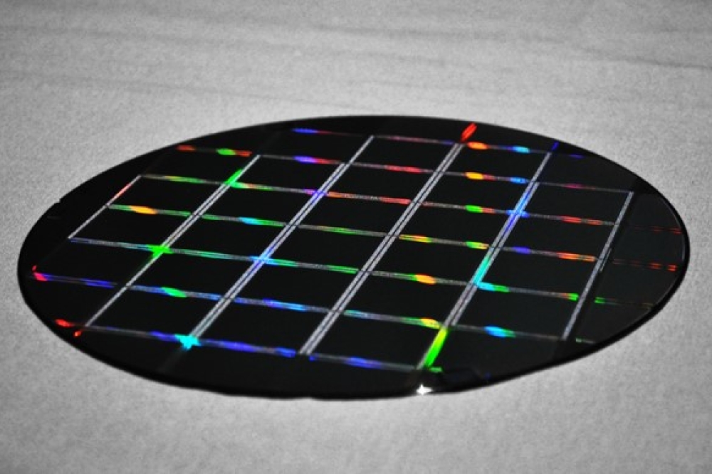
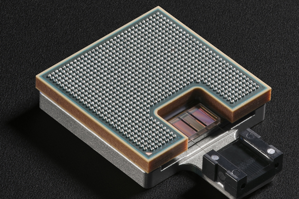
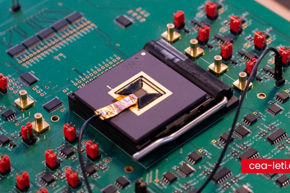
Vodafone’s engineers at its R&D centre in Málaga, Spain, are exploring the potential for new silicon photonic chips to become the hardware of choice to drive the customer-focussed mobile networks of the future.
The news that Vodafone is exploring this new technology comes as the company recently expanded its purpose-built campus in Málaga to house the more than 430 highly skilled engineers made up of over 30 nationalities already working there, along with the further 170 expected to join by 2025. In addition to advancements in silicon chip architecture, Málaga is home to Vodafone’s pioneering work in edge computing, IoT and network APIs, among other disruptive technologies, all of which support the digital transformation of Europe’s public sector and businesses of all sizes.
Far Faster Chips
Silicon photonic chips promise to be far faster, more efficient, and reliable than today’s electronic equivalent found in most electronic devices, including smartphones and telecommunications infrastructure. They use light instead of electricity to compute mathematical operations and the computation time is measured by how long it takes the light to cross the microchip.
The photonic chips would sit at the heart of Vodafone’s mobile base stations, providing an ultra-low latency, highly programmable and greener network. Their integration would support the massive advances in computation seen in new technologies like generative AI, cyber security (including quantum computing), and autonomous vehicles, to name but a few.
Vodafone’s engineers can predict the speed of a calculation based on the fact that light can travel seven and half times around the equator within one second, or in a one trillionth of a second (a picosecond) across a chipset. According to the University of Oxford, photonic chips could be three hundred times faster than electronic ones.
Working with Salience Labs and iPronics
Among the first start-ups to collaborate with Vodafone’s engineers at the expanded campus are two industry leading photonics companies - UK-based Salience Labs and iPronics, headquartered in Valencia, Spain. They join other vendors that are already working with Vodafone on the advancement of chip architecture to enhance new Open RANs.
Salience Labs and iPronics are assisting Vodafone in testing the latest silicon photonics, which has the potential to process and deliver huge amounts of data faster but still securely, without compromising the customer experience or requiring more masts.
Silicon photonics is becoming increasingly important because the increased demand for processing power from AI computer models requires more efficient and faster computer chips. AI computation alone is doubling around every three and half months, according to Salience Labs, and is outpacing what standard semiconductor technologies have left to offer.
Scaling up 5G
By taking a leading research role in silicon photonics today, Vodafone can ensure that it has the processing power baked into its network to match demand in years to come. It’s not only AI; scaling up new 5G features also requires a step-change in processing power at the mobile base station, for example network slicing where a business, hospital or school is given their own fast connection on demand.
Even though most microprocessors have reached their computing limit, they will more than adequately serve most electronic devices and networks for another 20 years. However, Vodafone is determined to stay ahead of the curve by looking to shape a new paradigm for compute with its partners.
Salience Labs is building silicon photonic solutions to overcome the challenge that the growth in AI presents to the movement of data in a world where traditional semiconductor technology can no longer scale higher to keep pace with innovation. Vodafone’s work with iPronics within the field of radio frequency beamforming – the ability to bend and direct a signal to its intended recipient such as a smartphone user – ensures that all aspects (the antenna and the actual baseband equipment) of a mobile base station are covered.
Driving Innovation in Europe
The just-in-time speed at which these silicon photonic chips make calculations will lead to fewer delays and far less heat generated in the transmission of data versus today’s method, which is reliant on slower and heat susceptible electronic capacitors. By collaborating with vendors such as Salience Labs and iPronics, Vodafone can drive silicon innovation in Europe and strengthen its position in the global market.


