Nokia joins innovation hub

Nokia to bring semiconductor expertise to CHIPS and Science Act funded innovation hub.
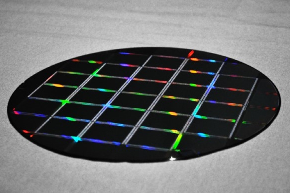
Nokia is part of the Northeast Microelectronics Coalition (NEMC) Hub, a regional innovation hub led by the Massachusetts Technology Collaborative (MassTech). The NEMC Hub was recently awarded funding to advance the microelectronics needs of the U.S. Department of Defense (DoD) from the "Creating Helpful Incentives to Produce Semiconductors (CHIPS) and Science Act." The funding award will establish a total of eight Microelectronics Commons regional innovation hubs and Core Facilities distributed across the United States, including NEMC, each focused on multiple technology areas and supported by a network of commercial innovators acting on a shared mission: to expand U.S. global leadership in microelectronics.
The DoD recently announced $238 million in funding that established the regional innovation hubs. This is the largest award to date under President Biden's CHIPS and Science Act. It will help make the American supply chain more resilient, safeguard the nation from supply chain risks and support national security and access to key technologies to keep America at the forefront of innovation and technological development.
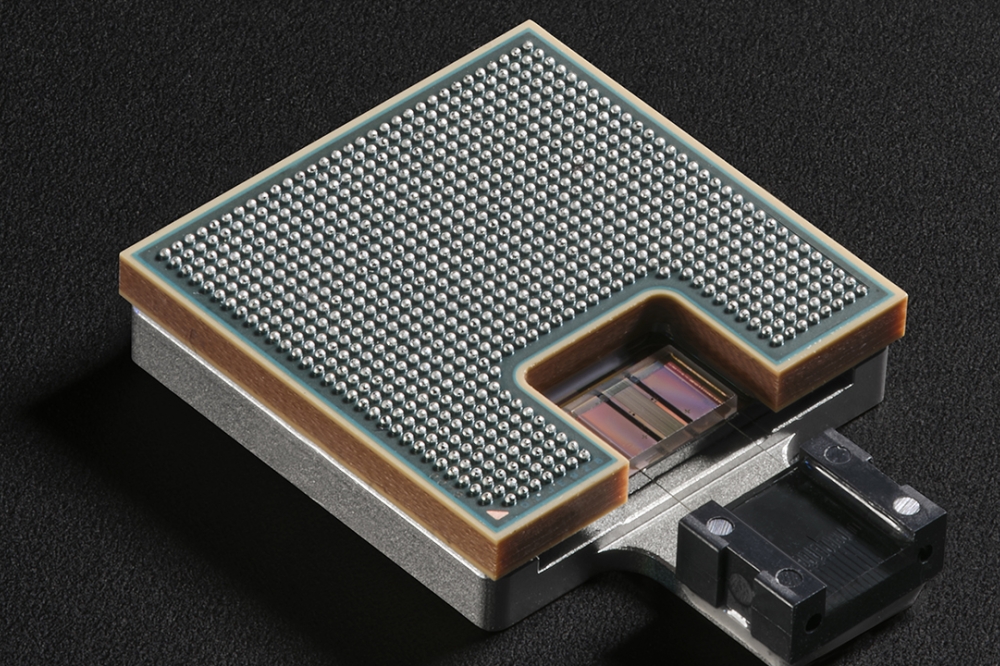
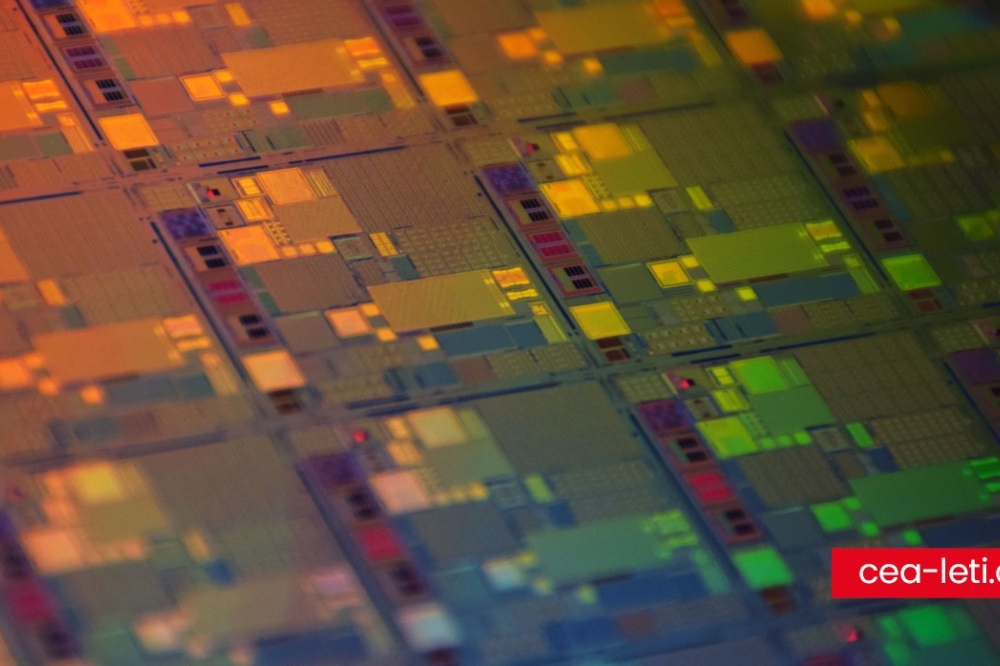
With $2 billion in funding for Fiscal Years 2023 through 2027, the Microelectronics Commons program aims to bridge the gap between R&D and chip production by leveraging the Hubs to accelerate domestic hardware prototyping and "lab-to-fab" transition of semiconductor technologies. This will help mitigate supply chain risks, ultimately expediting access to the most cutting-edge semiconductor electronics and photonics and creating a direct pathway to reduce America’s reliance on foreign microelectronics.
Nishant Batra, Chief Strategy and Technology Officer at Nokia, said: “Nokia is excited to be a key part of the Northeast Microelectronics Coalition Hub and apply our extensive experience in R&D to help accelerate U.S. semiconductor production. We are committed to ensuring U.S. scientific and industrial powerhouses have access to cutting-edge semiconductors and can deliver what is needed to secure future semiconductor needs while mitigating any future supply chain challenges.”
Carolyn Kirk, Executive Director of the MassTech Collaborative, said: “We are incredibly grateful for the trust and collaboration of our coalition members and the Department of Defense to establish and launch the NEMC Hub for the northeast and for the nation. Our selection demonstrates the power of partnerships and illustrates the immense talent that has come together to earn this designation.”
Building on Nokia’s recent announcements as the first telecom company to manufacture fiber-optic broadband network electronics products and optical modules in the U.S. for use in the Broadband Equity, Access and Deployment (BEAD) program and the first technology Buy America compliant vendor, Nokia is taking another important step with the NEMC collaboration to further contribute to U.S. technology leadership, economic growth, and job creation.


