X-FAB set to receive funding from the European IPCEI ME/CT

X-FAB Group is set to receive subsidies as part of the new Important Project of Common European Interest in Microelectronics and Communication Technologies (IPCEI ME/CT).
The funding, totaling up to 80 million Euros, is to be granted by the participating governments of France and Germany over a period of five years. The scheme supports innovation in microelectronics and communication solutions, playing a vital role in advancing European goals of digitalization, sustainability, and technological sovereignty.
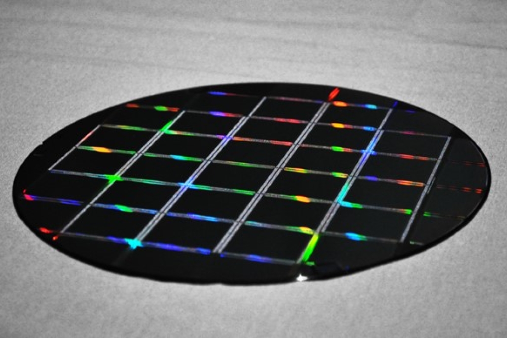
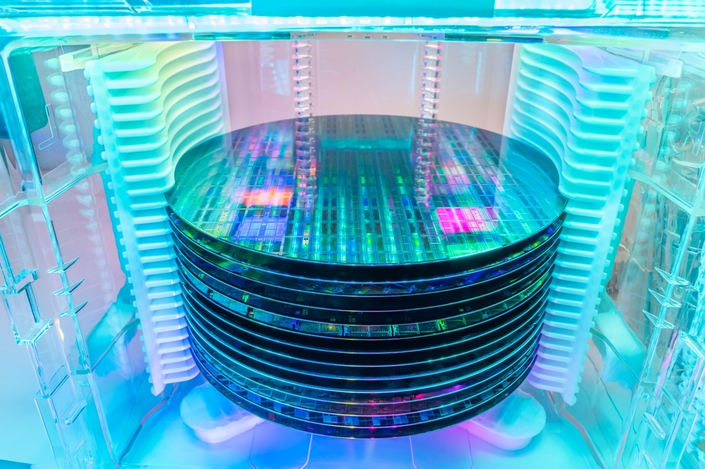
The funding will span across three of X-FAB's sites, each focusing on distinct aspects of semiconductor technology. The Corbeil-Essonnes facility in France specializes in smart sensors and drivers, new architectures, photonics and RF technologies. The site recently started volume production for 110nm technology on 200mm wafers, utilizing state-of-the-art BCD-on-SOI technology which was developed as part of the previous IPCEI ME program.
The Erfurt site in Germany researches and develops novel manufacturing platforms for smart integrated sensor systems, broadening X-FAB’s technology offering in smart sensor systems, 3D integration and heterogeneous chiplet integration through micro-transfer printing, thus further progressing cutting-edge technologies for system integration and advanced packaging.
At the Itzehoe site in Germany, X-FAB will focus on the development and implementation of new methods for processing glass wafers.
X-FAB recognizes the strategic importance of the IPCEI ME/CT funding in its efforts to develop differentiating technological offerings for next-generation semiconductor components. The initiative aims to meet the evolving demands of future markets in the automotive, medical, and industrial sectors, addressing needs including increased connectivity, smart sensors, and power devices with improved energy efficiency.
The funding will support a wide range of emerging technologies, serving a multitude of applications, including smart battery management, medical sensors, light sensors (such as LiDAR and OLED), communication devices compliant with future 6G standards, 5G mmWave, smart sensor systems, and microfluidic devices for biotech applications.
To achieve this, X-FAB is planning on collaborating with more than 40 key industrial partners, including SMEs and large companies, as well as academic institutions. These collaborations will cover various aspects along the semiconductor value chain.
“We express our gratitude for the IPCEI ME/CT funding, supporting research and development here at X-FAB. Our commitment lies in constantly pushing the boundaries of semiconductor technology. We are dedicated to delivering innovations that address key societal challenges, such as decarbonization, by advancing the transition to electric mobility and renewable energy sources, as well as providing dependable and efficient medical solutions to meet the needs of our growing and aging populations,” Rudi De Winter, CEO of X-FAB, notes.

