HKSTP and J2 Semiconductor sign MOU

R&D Centre at Hong Kong Science Park under the plan will conduct independent R&D and production of third-generation semiconductor chips.
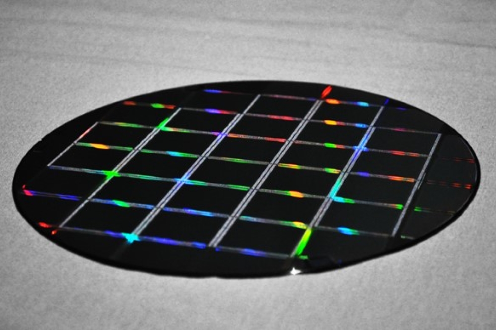
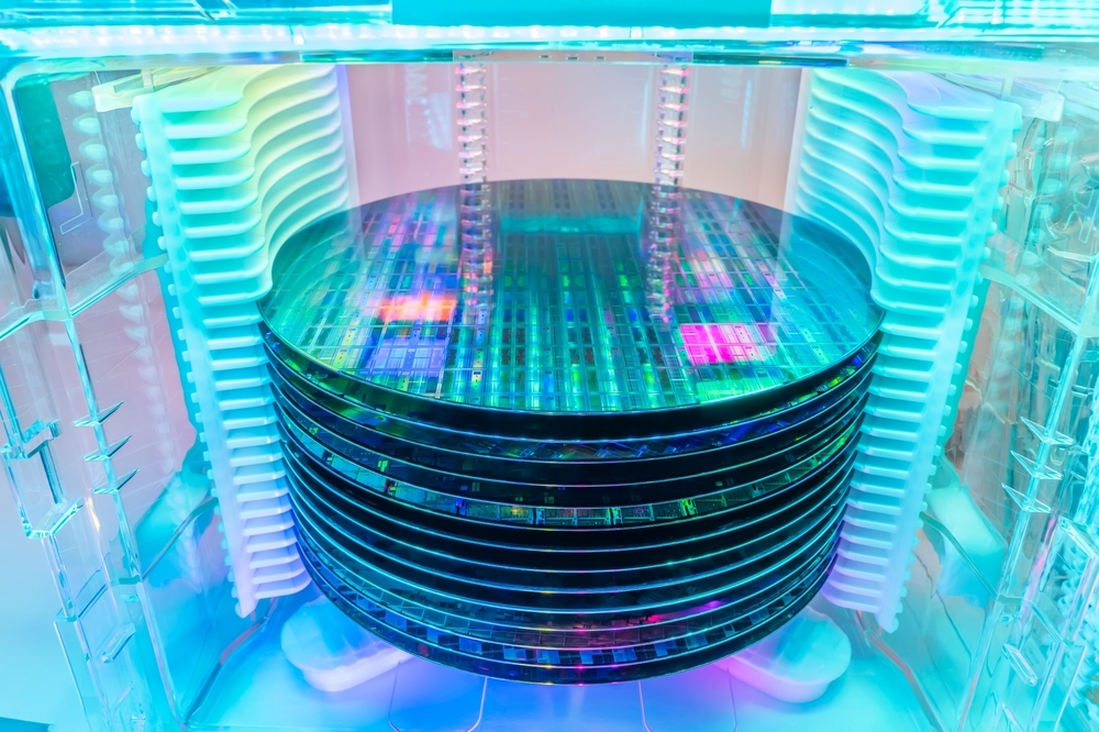
With support from the Innovation, Technology and Industry Bureau and the Office for Attracting Strategic Enterprises (OASES), the Hong Kong Science and Technology Parks Corporation (HKSTP) has signed a Memorandum of Understanding (MoU) with mainland China-based microelectronics enterprise J2 Semiconductor (Shanghai) Co. Ltd. (J2 Semiconductor), to set up a global research and development (R&D) Centre focusing on third-generation semiconductors at the Hong Kong Science Park, and to set up Hong Kong's first Silicon Carbide (SiC) 8-inch advanced wafer fab.
This is a milestone moment in the government’s ambition to establish Hong Kong as a leading microelectronics hub in the region. This further promotes new industrialisation, a core for the Innovation, Technology and Industry Bureau which published its “Hong Kong Innovation and Technology Development Blueprint", with a mission to develop strategically advanced manufacturing industries, such as microelectronics and semiconductors. As one of the world's largest import and export markets for semiconductors, Hong Kong is at the heart of the Greater Bay Area which offers huge potential in becoming a key hub in the global semiconductor supply and value chain.
Professor Sun Dong, Secretary for Innovation, Technology and Industry, said "This collaboration between HKSTP and J2 Semiconductor to set up the Hong Kong’s first-ever large-scale semiconductor wafer fab, demonstrates the commitment of the HKSAR Government in taking the initiative to turn its ‘new industrialisation’ vision into action. J2 Semiconductor is proactively building up the capacity, quality and competitiveness of Hong Kong’s tech talent pool. The project will also drive the development of related industries, including semiconductor equipment manufacturers, material suppliers, testing service providers, to develop a complete ecosystem to reinforce Hong Kong's position in the global semiconductor industry value chain."
The collaboration between HKSTP and J2 Semiconductor is jointly supported by the Innovation, Technology and Industry Bureau and OASES with a view to sustain Hong Kong's innovation and technology ecosystem and promote new industrialisation. The MoU was witnessed by Professor Sun Dong, Secretary of Innovation, Technology and Industry Bureau, Mr Philip Yung, Director-General of OASES, Ms Lillian Cheong, Under Secretary for Innovation, Technology and Industry, Dr Sunny Chai, Chairman of HKSTP and Dr Robert Tsu, Chairman of J2 Semiconductor. While Mr Albert Wong, CEO of HKSTP and Mr TY Chu, Co-CEO of J2 Semiconductor formally signed the MoU.
Dr Sunny Chai, Chairman of HKSTP said, "The plan of establishing J2 Semiconductor’s R&D Centre in the Science Park will promote Hong Kong's R&D and advanced manufacturing capabilities of third-generation semiconductor devices. J2 Semiconductor brings the core technology and expertise to Hong Kong in advanced chip design, fabrication process and semiconductor product development, which is an important milestone in the development of microelectronics industry in Hong Kong. As one of Hong Kong's flagship innovation and technology platforms, we provide high-quality infrastructure and facilities as well as a vast network of partners, which will continue to promote Hong Kong's microelectronics R&D capabilities and strengthen Hong Kong's position as an international I&T hub."
Dr Robert Tsu, Chairman of J2 Semiconductor said, “I am very grateful for the level of attention and support from both the Innovation, Technology and Industry Bureau and HKSTP to this project. The MoU signing officially launches our third-generation semiconductor ‘SiC 8-inch advanced wafer fab’ project. J2 Semiconductor will invest an estimated HK$6.9 billion into the project, with plans to start volume production in the next couple of years, and reach annual production capacity of 240,000 SiC wafers in 2028, generating an annual production value of more than HK$11 billion and creating more than 700 job positions in Hong Kong. The project will assist in the early completion of the localisation of the new energy vehicle supply chain and drive the long-term development and prosperity of the semiconductor industry in Hong Kong.”
As a semiconductor chip design enterprise, J2 Semiconductor is committed to meeting the strong demand for domestically produced automotive chips from the China automotive industry. It mainly provides high-performance silicon carbide (SiC) devices with a focus on automotive, power conversion and communications. J2 Semiconductor’s SiC technology can be applied to relevant applications such as electric vehicles, as well as the related infrastructure such as charging stations, smart grids and energy storage.
HKSTP is committed to promoting Hong Kong's new industrialisation mission and building a world-leading microelectronics ecosystem. HKSTP has established an extensive network of microelectronics hardware infrastructure, including Sensor Packaging and Integration Laboratory (Sensor Lab), Heterogenous Integration Lab (HI Lab) and the Hardware Lab, which can support the end-to-end process of design, prototyping and pilot production of chip-related equipment and systems as well as products. The Microelectronics Centre in Yuen Long Innovation Park is set to begin operation in 2024, supporting HKSTP's infrastructure to accelerate microelectronics R&D pilot production, creating opportunities for upstream and downstream enterprises in the industry chain.
The microelectronics ecosystem of HKSTP is flourishing, with more than 200 microelectronics related companies. The establishment of the J2 Semiconductor facilities in Hong Kong will create greater level of synergy and knowledge exchange. Currently, five universities in Hong Kong are ranked among the top 100 universities in the world, with more than 100 university researchers engaged in microelectronics research, and promote the R&D of third-generation semiconductors. In this year's Budget Speech, the HKSAR Government announced its plan to establish a Microelectronics Research and Development Institute to strengthen collaboration with universities, R&D centres and companies in the industry, and further accelerate the "1 to N" translation of R&D outcomes and bolster industry development.

