+44 (0)24 7671 8970
More publications     •     Advertise with us     •     Contact us
 
Loading...
News Article

Ansys solutions certified for UMC's 3D chip technology

News

Ansys semiconductor simulation tools are certified for UMC's latest wafer-on-wafer (WoW) advanced packaging technology.

Ansys multiphysics solutions have been certified by global semiconductor foundry UMC to simulate its latest 3D-IC WoW stacked technology, which will improve the power, efficiency and performance of edge AI, graphic processing, and wireless communication systems. The certification empowers more chip designers to employ Ansys’ semiconductor simulation solutions that perform multi-die co-analysis for streamlining and ensuring successful design.

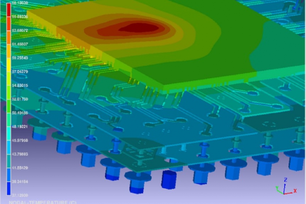
WoW technology consists of silicon wafers, or dies, that are stacked vertically rather than placed horizontally across a board. Built on cloud-optimized infrastructure, Ansys RedHawk-SC™ and Ansys RedHawk-SC Electrothermal™ have the speed, capacity, and predictive accuracy to handle full-chip analysis, including multi-die packages and interconnects for power and signal integrity, thermal profiling, and more. These 3D-IC solutions for multiphysics analysis fit into a larger set of comprehensive Ansys solutions for board and system electrothermal analysis, including Ansys SIwave™ and Ansys Icepak™.

“We’re pleased with the result of our collaboration with Ansys in the delivery of UMC technology reference flow, which empowers customers to address growing performance, reliability, and power demands for cloud and data center applications,” said Osbert Cheng, vice president of device technology development and design support at UMC. “The collaborative efforts combining Ansys’ comprehensive chip-package co-analysis solutions with UMC’s advanced chip-stacking technology address complex multiphysics challenges in 3D-IC packaging technologies.”

“Ansys and UMC’s 3D-IC solutions address complex multiphysics challenges to meet stringent power, performance, thermal and reliability requirements,” said John Lee, vice president and general manager of the electronics, semiconductor, and optics business unit at Ansys. “Ansys’ dual-approach with both chip- and system-aware design solutions enable mutual customers to accelerate design convergence with greater confidence from small, delicate details at chip level to system-level design challenges.”

Reality AI Explorer Tier offers free AI/ML development access
AEM introduces new generation of Automated Burn-In Systems
NPUs are emerging as the main rival to Nvidia’s AI dominance, says DAI Magister
Camtek receives a $20M order from a Tier-1 OSAT
Free samples of every STMicroelectronics NPI IC available from Anglia
NY CREATES and SEMI sign MoU
Major government investment to 'propel' Canada
QuickLogic announces $5.26 million contract award
ASNA and Athinia collaborate
Global sales forecast to reach record $109 billion in 2024
AMD to acquire Silo AI
Nanotronics unveils 'groundbreaking' Gen V AI Model
Aitomatic unveils SemiKong
Biden-Harris Administration reveals first CHIPS for America R&D facilities and selection processes
Collaboration to produce cutting-edge AI accelerator chips
Oxford Ionics breaks global quantum performance records
Adeia wins ECTC Award for paper on “Fine Pitch Die-to-Wafer Hybrid Bonding”
AEM introduces new generation of Automated Burn-In Systems
Sydney council forges vital semiconductor agreement
EV Group's EVG880 LayerRelease wins 2024 Best of West
Biden-Harris Administration to invest up to $1.6 billion
Cyient sets up subsidiary for semiconductor business
EMD Electronics network leaders honoured
Accenture acquires Cientra
Introducing Park FX200
Deep learning chipset market to surge to $72.8 billion by 2033
PI Innovation Award 2024: Nanobodies for Diagnostic and Therapeutic Applications
Graphcore joins Softbank Group
Kaman Measuring highlights high precision displacement sensors
Si2 reveals recipients of Annual Power of Partnerships Award
Advantest achieves ASPICE Level 2 Certification for V93000 SmarTest 8 Software
Semiconductors to become a trillion-dollar industry by 2030
×
Search the news archive

To close this popup you can press escape or click the close icon.
Logo
×
  • 1st January 1970
  • 1st January 1970
  • 1st January 1970
  • 1st January 1970
  • 1st January 1970
  • 1st January 1970
  • 1st January 1970
  • 1st January 1970
  • View all news 22645 more articles
Logo
×
Register - Step 1

You may choose to subscribe to the Silicon Semiconductor Magazine, the Silicon Semiconductor Newsletter, or both. You may also request additional information if required, before submitting your application.


Please subscribe me to:


You chose the industry type of "Other"

Please enter the industry that you work in: