
Taking testing to the next level
EMANUELE BARDO, VICE PRESIDENT FOR THE SEMICONDUCTOR AND MEMS TEST BUSINESS UNIT AT SPEA, talks to Silicon Semiconductor Editor, Philip Alsop, about the company’s Automatic Testing Equipment expertise as it relates to the semiconductor sector, highlighting technology innovations, alongside the company’s future growth plans.
SPEA was founded in North Italy in 1976. The founder worked for the famous Italian company, Olivetti, and later on with General Electric, before founding SPEA. The initial business was related to the production of ICT testers - testing of assembled PCBA boards.
In 1993, SPEA produced its first semiconductor tester, that went into the market a year later. Being European, the first installed base was with the major semiconductor IDM companies here in Europe. The company’s first high volume semiconductor tester went out in the market in 1999 and later on with a second version in the 2002/2003. SPEA then penetrated the sensors’ market in 2003/2004. At the time, there were not many applications. One early successful application was the Nintendo Wii, that contained the first three axial accelerometers - which were tested and calibrated with SPEA machines. Since then, the consumer business has driven a lot of innovation in the sensor business, followed by the automotive industry.
In 2009/2010 SPEA started to heavily penetrate the high voltage and high current business that today represents one of the biggest revenue shares of the company, driven again by automotive and electric cars. And in 2018, SPEA was able to introduce the second generation of what it calls the DOT device-oriented tester. And this has been one of the biggest ‘revolutions’ in the industry, introducing a new way of conceiving the ATE that represents an extremely successful business case for a lot of customers in Europe, in the United States, in Asia - in Korea, in Japan and in mainland China. Today, the company has a turnover that is over 200 million euros, and the target is to break the 300 million euro barrier in the next two years.
In terms of how the company positions itself within the automatic test equipment market, it is currently in the number four position. However, the company is dominant in two major markets. In the MEMS sensors market, the company has more than 60% of the market, and also has a significant presence in the high voltage and high current semiconductor product market. The big news is that, on the analogue mixed signal side, that was dominated by its two major competitors in the past, SPEA’s market share has more than tripled in the last four years. With the company’s machine designs bringing down the cost of test in a significant way, based on its four year roadmap, SPEA expects to move up to the overall number three market position.

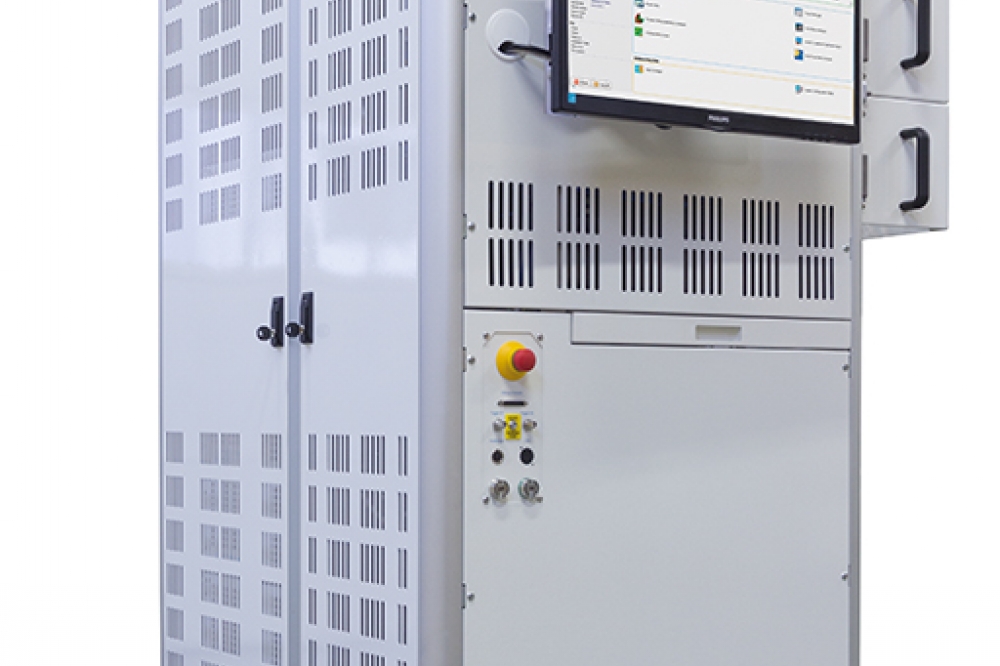
The innovative DOT test platform addresses the test requirements of
applications like BMS, SerDes, OpAmp, PMIC, MEMS and sensors,
Microcontrollers.
In terms of how SPEA distinguishes itself in the market, what it does differently from the competition when it comes to semiconductor testing, Emanuele explains: “Measuring a voltage and measuring a current is equal for all the ATE vendors. Of course, if you have to measure five volts with a certain accuracy, or you have that spec, or you don’t have, the key is how you do it and how you make this cost efficient. To make things cost efficient today, you have to work on two major topics - design architecture and distributed intelligence in the machine. So, the architecture of the machine brings to two major advantages - to have an equipment that is extremely modular and configurable in a way that the overall Capex cost is significantly lower than the competitor. The second topic is how you design your instrument, your backplane in order to get the highest multi-site efficiency - semiconductor tests require multi-site testing for cost proposal. So, the key question is how much is the percentage of test time increased every time you add one site during the parallel test? So, if your efficiency is 99, that’s an okay number, but if your efficiency is 99.95%, that’s a different number and that represents cost saving. So, these two elements are driven by the architecture of this test.”
Emanuele continues: “The other topic is the intelligence that you put inside the machines today. This type of equipment - they use their own intelligence to self-control their own calibration data in order that automatically the machines can recalibrate on the fly in the spare time they have on the production floor. This is coming away from the old model of working where you have the equipment and the tester operating for a certain amount of hours then going into a preventive maintenance operation, then doing diagnostic and calibration and so on.

The DOT800 test platform incorporates the elements of Industry 4.0, in
terms of auto-maintenance capabilities, data collection and analysis,
and artificial intelligence in the service of an easy test program
migration from legacy testers.
“The big advantages that we are introducing are exactly these three, the architecture, multi-site efficiency and intelligence in the equipment. Overall, this represents cost saving. And when you start to slice the cost in different portions and you act on all of this in parallel, you are able to cut those costs by a significant percentage. That’s the competitive element and why a big customer would consider changing their test platform.”
In terms of SPEA’s product and services portfolio, the DOT tester is the biggest innovation. DOT means device-oriented tester and the name itself represents a big step forward for the company’s architecture because the old ATE machines, they used to have purely analogue cards, purely digital cards, single processing cards, high voltage cards and so on. The customer was selecting equipment, it was coming out of the budget and it was demanding their application team to rail out a PCB interface to specialise the tester interface to the product.
With the DOT, SPEA has boards that are themselves configurable. So, the customer knows his product portfolio and he can configure one board with a logic mixing of analogue, digital, signal processing and power in a way that with one card the customer can test one, two, four or eight devices in parallel
and then populate the tester with the required number of the same card. This is the big cost advantage and the technical element that brings us to multi-site efficiency. So, this is one of SPEA’s major elements on the mixed signal tester side.
The company also has a very strong technological roadmap on everything relating to power - high voltage, high current. This market, that was a very low market until three years ago, is now booming. And even during 2023, in a year where generally the semiconductor industry market is going down, the only market segment that has two-digit growth is power and discrete - driven by automotive, by the EV car, by the hybrid car, by the charging stations. In this market segment, SPEA is extremely advanced because it is partnering with important IDM companies and is hitting all the voltage standards and the required accuracy. So, these two segments are the ones in which the company is investing more at the moment.
At the SEMICON West, SPEA introduced one or two innovations. The event was a very positive one for the company - the United States market that really ‘requires innovation from a new supplier coming out from the monopoly of the old ATE suppliers’. In terms of the architecture aspect already mentioned, SPEA has developed ultra-high speed digital pins that will become an option for the low cost mixed signal tester, with the concept that you can configure one of the cards partially with a high speed digital pin. In terms of all the products that you have today, they have high speed interfaces like Ethernet, HDMI and so on.
To bring the cost of test low for high-speed digital testing has always been a big challenge and with this type of innovation, SPEA offers the option to configure a channel board with low speed digital, high speed digital, analogue and signal processing, at a very competitive cost . And this is related to the mixed signal.
The other big topic that the company discussed at SEMICON West was the emerging needs of the silicon carbide product testing, where the voltage ratings are going above 3000 volts and as possible roadmap above 6000 volts.
Another significant innovation that SPEA introduced recently focuses on auto maintenance. Emanuele explains: “The old ATE systems, they work in a way that they operate a certain amount of hours, then they go into a preventive maintenance mode and the machine has to do calibration adjustment and eventually also diagnostics. What we have been able to do is to know when the tester has idle time. If you do a calculation, this time is very significant during one month. Well, we are capable to understand when the tester is idle for a certain amount of time.
“At that point, we can run a subset of our calibration programme in order to verify the drift of the calibration data. We are able to keep track and memory of this data over the time. And we are capable to predict when an instrument potentially can go out from the calibration thresholds. And at that point, when we have that prediction, instead of setting the tester in PM with an appropriate margin, we are able to auto recalibrate the machine.”
This auto maintenance/calibration innovation is industry 4.0 in action – making the tester smart enough so it can automatically control drifting of the data and eventually recalibrate.
Another function that SPEA has introduced in terms of Industry 4.0 is to develop a tester that is capable of calculating the lifespan of relays. All ATE is full of mechanical and solid-state relays. These are parts that sooner or later will fail because they have a certain lifetime. Being able to understand what is the lifetime of the consumable parts that are mounted in a tester and being able to predict end of life represents a very important advance, because it helps customers to reduce downtime and to improve their manufacturing efficiency.
And from Industry 4.0 to artificial intelligence and machine learning is but a small step, as Emanuele acknowledges: “AI will bring a lot of potential in the future and I think the potential will be for a supplier like us to help our customers with migration of the test programme and the test application from one machine to another. As I said earlier, we are coming later to the market and we offer a competitive advantage, but one of the big headaches for our customer is oh, we have already many products running on machine A, we need to convert on the SPEA. Using AI to help during this test programme migration will be a big opportunity in the future.
“This will be the next step forward where we can give a huge advantage to our customer. And our design team and our software team are working on this topic, because it’s not only matter of the AI itself, but it’s also a matter of how we design our software architecture to make that friendly in a way that the migration can be done automatically using AI tools with the appropriate level of confidentiality the customer wants to have.”
While the ubiquitous confidentiality agreements which surround the semiconductor industry prevent Emanuele from sharing details as to how SPEA is helping specific companies, he is able to give a high-level view of the type of work which is being undertaken.
Emanuele says: “In the last two years, we have played an extremely important role in everything to do with BMS (Battery Management System) testing. We have helped a major customer to reduce more than 50% of their operating cost thanks to the use of dedicated instrumentation, with extremely high accuracy, that we have developed for this business. You can understand that doubling the output with our existing machine, together with all the advantages I mentioned before, is a huge cost saving, floor space saving and the like. This is one of the biggest successes that we have achieved.
“We have also supported another major customer with sensor testing, where they were able to gain an extremely big market share thanks to our multi-site capability that was ten times higher than our competitor. These are two very nice examples of partnerships that we have built over the years and which have brought a lot of advantages to two of our major customers.”
Looking to the future, Emanuele expects SPEA’s organic growth to continue across all sectors. The rate of growth is biggest in the analogue mixed signal space and in the power space – they are very big market segments and also the market segments where SPEA is focusing introducing the majority of its innovations.
The sensor business is still growing, but not at the same rate of previous years. That said, the sensor business is growing in an impressive way in mainland China where SPEA plays a dominant role and has recently set up partnerships.
The high growth in the analogue mixed signal and the high-power segments brings many challenges for the company. SPEA has recently approved a massive investment that will increase capacity by more than two and a half times the current output over the next two years and beyond.
Emanuele summarises: “This is a massive investment, not only in our headquarters here in Italy, but all over the world. Because, of course, we are growing our organisation in all the countries from Asia, China, Southeast Asia, United States and Europe. By growing our installed base, our customers need faster answer times, they need application capability, they need service capability, they need local repair centres. That’s where all the investments will be focused - to be as close as possible to the customer.”
In terms of the technology future, SPEA has a five year roadmap, from both a hardware and software perspective. The company shares its plans with, and receives regular feedback from its major customers as to their own plans – where they are going. It also works with individual customers to validate innovations. Emanuele explains: “Recently, we have also introduced the following practice: once we introduce a new piece of equipment or a new equipment feature, we work together with a customer to identify one of their products that has a specific technical requirement for the innovation and we work together to shorten the validation time and to speed up time to market in an improved way with a fully validated solution.”


