
Intel's Oregon investments fuel US innovation
Intel's commitment elevates the ‘Silicon Forest’ as a global semiconductor R&D and manufacturing hub, strengthening the region’s economic growth.
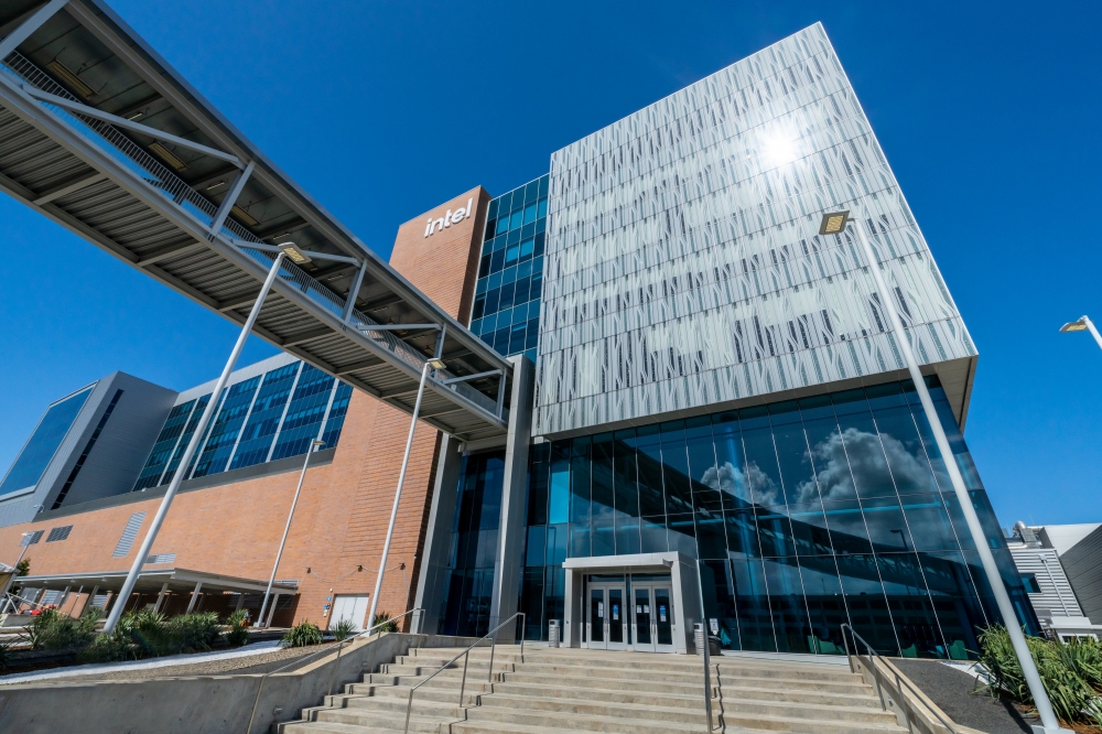
Intel recently shared its plans to advance its semiconductor technology development facilities at the Gordon Moore Park at Ronler Acres in Hillsboro, Oregon. The campus is Intel’s innovation hub for leading-edge semiconductor research, technology development and manufacturing in the United States. This undertaking is possible with support from the state of Oregon, city of Hillsboro and Washington County, and in anticipation of support from the U.S. CHIPS and Science Act.
Dr. Ann Kelleher, Intel executive vice president and general manager of the Technology Development Group comments: "Intel has been dedicated to driving innovation and advancing technology in Oregon for almost five decades, and we are set to lead the charge in restoring America's leadership in semiconductor R&D and manufacturing, backed by Oregon and the U.S. CHIPS Act. This investment further solidifies our commitment to the Silicon Forest and rebalancing the global semiconductor supply chain.”
The investments in Intel’s Oregon R&D and manufacturing operations are pivotal to the company’s technology leadership goals. They are part of Intel’s plans to invest more than $100 billion in the U.S. over a five-year period, CEO Pat Gelsinger said at September’s Intel Innovation event.
Plans include:
• Ongoing advancement of the company’s existing technology development facilities at the Gordon Moore Park campus. This substantial upgrade will usher in the latest in process technology and tools, putting the campus at the forefront of innovation.
• The world’s first high-numerical aperture extreme ultraviolet (high-NA EUV) lithography tool is planned to dock this year.
• Initiation of the application process for permits to enable a potential future multibillion-dollar expansion to Intel’s R&D and manufacturing capacity.
These investments, comparable to investments being made in other U.S. Intel sites and contingent on support from the U.S. CHIPS Act, would support several thousand new permanent and construction jobs and help ensure that Oregon and the Pacific Northwest remain the hub of U.S. semiconductor R&D and technology development for years to come.
Oregon Gov. Tina Kotek recently joined Intel executives in Hillsboro in celebration of Intel’s major commitment and in support of the company’s unified vision for driving future innovation, technology development and manufacturing capabilities in the state.
"Intel's significant investments in Oregon reflect a shared vision of success and innovation,” Kotek said. “As the governor of this great state, I am excited about the positive impact that Intel's expansions and partnerships will have on Oregon's technology landscape and the future of our workforce. This collaboration highlights our state's commitment to fostering economic prosperity and diversity through education and innovation."
Intel says that it is the only leading-edge semiconductor manufacturer that headquarters its R&D and technology development in the U.S. Oregon plays a pivotal role in Intel's strategy to regain process technology leadership by 2025 and fulfill the company’s IDM 2.0 strategy. Support from the state of Oregon, city of Hillsboro and Washington County has helped make this possible. Additionally, incentives from the U.S. CHIPS Act have the potential to significantly accelerate advancements at the site and help ensure the U.S. retains leading-edge semiconductor technology capabilities long into the future.
Intel remains committed to delivering five nodes within four years and regain process technology leadership by 2025. Intel is making good progress on its roadmap, recently achieving a significant milestone with the commencement of high-volume manufacturing of Intel 4 technology in Ireland.
Intel’s facilities in Hillsboro, Oregon, are at the core of the 'most important' semiconductor innovation cluster in the United States. The company relies on strong partnerships with the city, county and state, as well as with the construction trades, educational institutions and local nonprofits. In remarking on the strength and unity of the varied ecosystem stakeholders during her visit to Oregon on April 5, 2023, U.S. Commerce Secretary Gina Raimondo stated that she was “blown away” by the way Intel, the community and government came together to help fuel the semiconductor industry in Oregon.
Oregon is the home to Intel’s Technology Development Group. The group’s research teams are looking 10 or more years into the future to envision new process technologies. Simultaneously, Intel’s teams are driving efforts to minimize the company’s environmental footprint by identifying greener chemistries and treatment strategies. These efforts will help Intel achieve its commitment to net-zero greenhouse gas emissions across its global operations by 2040.
Intel is working to further increase access to opportunity, empower the next generation of innovators and expand its industry talent pool. Investments in programs across the state, in collaboration with universities, community colleges and local school districts, underscore Intel’s commitment to STEAM education and accessible workforce pathways.


