
Leading edge semiconductor research on 200/300 mm wafers
Modern electronics developments require state-of-the-art technologies and manufacturing processes, which are a financial challenge for many companies.
Located in the heart of Silicon Saxony, Fraunhofer Institute for Photonic Microsystems IPMS offers both large chip manufacturers and smaller companies access to the latest research results and technologies on 200 and 300 mm silicon wafers. Services range from consulting and process development to pilot production. Green ICT - i.e. sustainability - is also playing an increasingly important role.
MEMS technologies and devices on 200 mm wafers
At Fraunhofer IPMS, the technological development and support of MEMS technologies is carried out along the entire value chain: from individual processes to technology modules to complete technologies, as well as the process-technological support of the equipment in the cleanroom. i. After successful development, the institute offers pilot production or support for technology transfer. Fraunhofer IPMS covers the technological maturity levels (TRL) from three to eight. Especially start-ups, SMEs and companies without their own fab can thus benefit from low investment costs.
In the field of sensors and actuators, Fraunhofer IPMS develops, for example, capacitive ultrasonic sensors. These are offered as a platform for rapid customer-specific adaptations. This provides small and medium-sized companies with cost-effective access to high technology.
Another important aspect for customers: A simple and cost-effective way to test the latest developments in their application. For this purpose, Fraunhofer IPMS offers evaluation kits. With these ready-to-use setups, customers can, for example, immediately integrate the microscanner technology into their product development, since the appropriate control electronics according to the specifications are already included in the scope of delivery. Costly in-house development is no longer necessary.
300 mm semiconductor process and product development for nanoelectronics
With the Center Nanoelectronic Technologies (CNT), Fraunhofer IPMS conducts applied research on 300 mm wafers for chip manufacturers, suppliers, equipment manufacturers and R&D partners.
A wide range of technology development and support services are offered in the area of Ultra-Large-Scale Integration (ULSI). These include individual process developments in the areas of atomic layer deposition, chemical-mechanical polishing, wafer metallization, wafer cleaning, metrology and nanopatterning. The CNT's cleanroom is also used to evaluate and optimize chemicals and consumables for the latest CMOS technologies and to qualify equipment. The main focus of R&D activities is in the front-end area with a focus on the integration of functionalities in wiring layers (BEoL module). This mainly includes various non-volatile memories, capacitors or varactors. Together with Fraunhofer IZM-ASSID (focus on heterointegration and wafer level packaging), competencies are bundled in the center CEASAX (Center for Advanced CMOS & Heterointegration Saxony) and research is focused on neuromorphic computing, cryo- and quantum technology as well as advanced packaging.
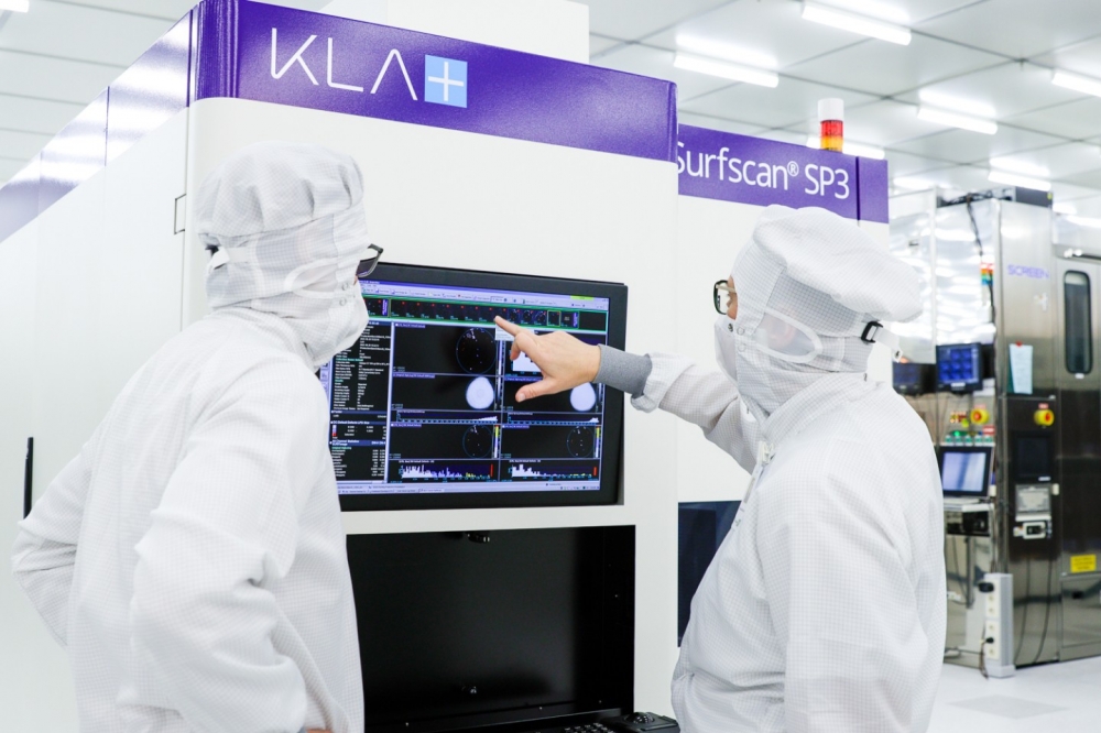
To expand the possibilities, a technology center for semiconductor metrology and process analysis was founded with the company Applied Materials. For this purpose, state-of-the-art eBeam metrology equipment from Applied Materials has been installed at Fraunhofer IPMS. Precise metrology is crucial for quality control in the production of microchips to validate physical and electrical properties and to ensure the targeted yield.
Green ICT - Sustainable information and communication technology
Increasing digitalization presents both opportunities and challenges for environmental protection. The intelligent control of devices saves energy, but the continuing proliferation of these devices increases energy consumption. Microelectronics therefore needs new approaches to minimize the environmental impact in both manufacturing and design. Fraunhofer IPMS is working closely with Research Fab Microelectronics Germany (FMD) in the Green ICT competence center to actively promote the reduction of resource consumption. This includes energy-efficient sensor edge cloud systems (battery-free sensors and neuromorphic AI accelerators) and communication devices (Li-Fi and Ethernet TSN) as well as resource-optimized electronics production on 200 mm and 300 mm wafers. The latter includes optimization of material consumption and substitution of critical materials in wet processes and lithography, as well as optimization of energy consumption and emissions impact.


