
Silicon Austria Labs and EV Group strengthen collaboration
Credit: Silicon Austria Labs
EV Group (EVG), a supplier of wafer bonding and lithography equipment, and Silicon Austria Labs (SAL), an Austrian research centre for electronic based systems (EBS), have strengthened their collaboration on heterogeneous integration.
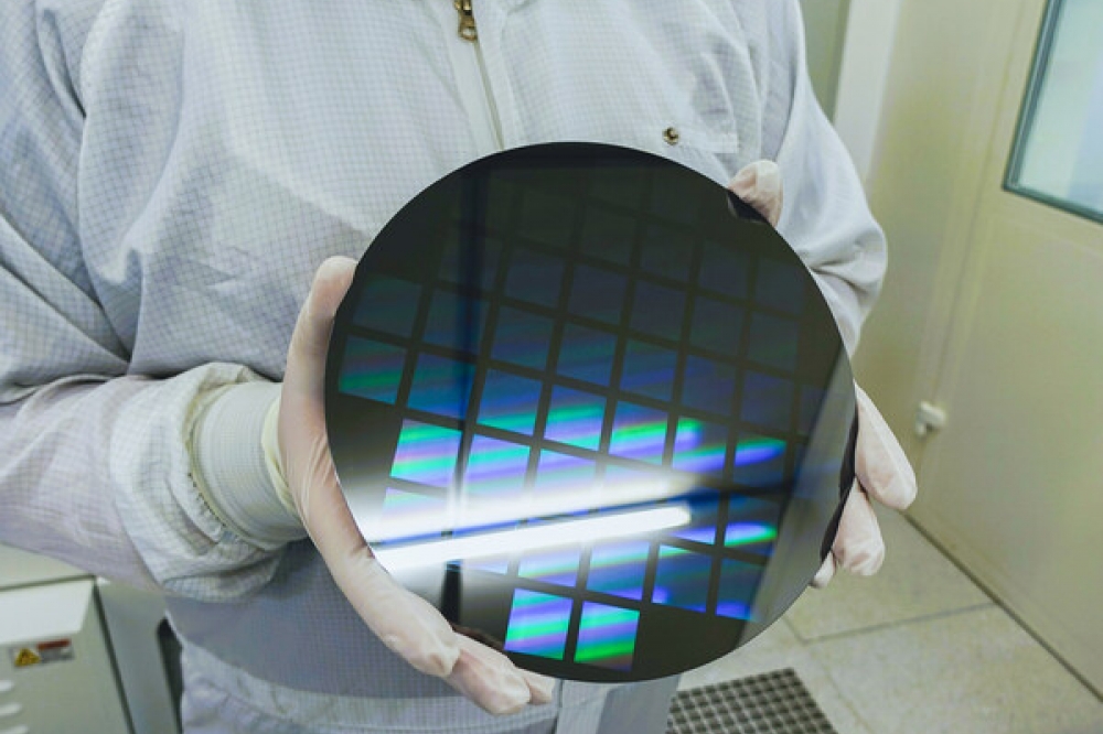
As part of this cooperation, the organisations have announced that SAL has received and installed multiple EVG lithography and resist processing systems at its MicroFab R&D cleanroom facility in Villach, Austria. Together, the companies seek to accelerate the development and deployment of advanced optical technologies for heterogeneous integration applications, including wafer-level optics used for micro cameras and micromirrors, diffractive optics, and automotive optics used to enable autonomous driving and automotive lighting.
The newly installed EVG systems include the LITHOSCALE maskless exposure system, the EVG7300 automated SmartNIL nanoimprint and wafer-level optics system, as well as multiple complementary resist processing systems. These systems join SAL's existing installed base of multiple EVG bonding, mask alignment and lithography systems, including the first installation of the next-generation 200 mm version of the EVG150 automated resist processing system. EVG says the latter provides significantly higher throughput, increased flexibility and smaller tool footprint compared to the previous-generation platform.
In addition, SAL has been working closely with the technology development and application engineering team at EVG's headquarters, including the NILPhotonics Competence Center, to leverage EVG's equipment and process knowhow and develop processes that are transferable and scalable to high-volume manufacturing.
Dr. Mohssen Moridi, head of the Microsystems Research Division at SAL, said: "We have recently been immersed in a range of cutting-edge R&D projects spanning meta-optics, integrated photonics, and MEMS, necessitating the use of advanced lithography and bonding tools. Through our valued partnership with EVG, we have gained access to tools of exceptional reliability and precision, paramount for successful R&D endeavours. Notably, the EVG7300 SmartNIL system has emerged as a pivotal tool, enabling the mass production of nanostructures for emerging photonics and MEMS devices. Its applications extend to diverse fields such as smart lighting systems, AR/VR, automotive optics, telecommunication, and quantum technology."
SAL was among the first customers to receive the new EVG7300 system, which EVG says is its most advanced solution combining multiple UV-based process capabilities, such as nanoimprint lithography (NIL), lens molding and lens stacking (UV bonding), in a single platform. The EVG7300 was developed with the intention of serving advanced R&D and production needs for a wide range of emerging applications involving micro- and nano-patterning as well as functional layer stacking.
Thomas Glinsner, corporate technology director at EV Group, added: "Silicon Austria Labs is a leading research centre for optical miniaturisation and heterogeneous integration, and is a strategic partner for EV Group. This latest shipment and installation of our advanced lithography and resist processing systems further strengthens our relationship and supports SAL's ability to develop future key technologies and apply our leading-edge solutions into real-world industrial applications."


