
KYOCERA Fineceramics Europe doubles its production capacity in Germany
The subsidiary of KYOCERA Europe GmbH, which is part of the Japanese Kyocera Group, is aiming to become the market leader in Europe and is focusing on bringing about a green transformation at its two manufacturing sites in Mannheim and Selb.
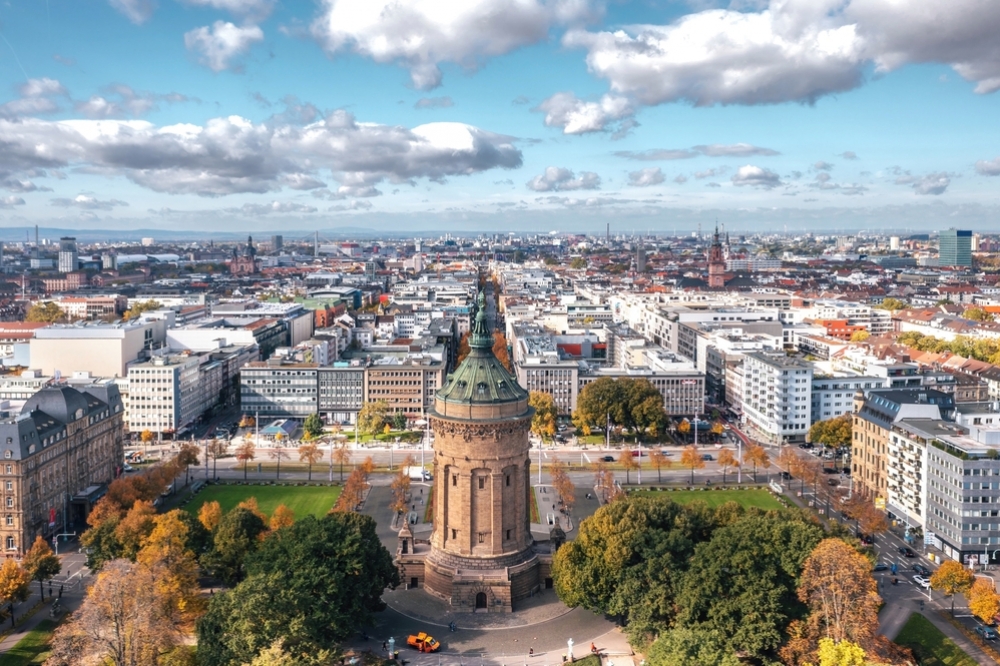
Kyocera Fineceramics Europe GmbH plans to invest around 34 million euros in its two European sites in Mannheim (Baden-Württemberg) and Selb (Bavaria) in the current 2023/24 financial year. This is yet another example of how important Germany is to Kyocera as an industrial location and a driving force for the entire European market. KYOCERA Fineceramics Europe GmbH is one of the world’s leading suppliers of advanced ceramics for a wide range of industrial applications, ranging from automotive to energy and medical technology to semiconductor manufacturing.
“The challenges of industrial transformation in Germany are enormous. Especially so in an energy-intensive industry like ours. That is why linking commercial aspects and green issues is particularly important to us. This is exactly what these investments are designed to achieve,” explains Dr Carsten Rußner, President of KYOCERA Fineceramics Europe GmbH.
Sustainable investments in buildings, facilities and employees
Demand for Kyocera’s products is high and the order books are very healthy. The company wants to continue its growth. There is a clear growth strategy in place to achieve this: “The Kyocera Group does not focus on short-term shareholder value effects. For us, the long-term perspective is what counts: we want to become the No.1 in the European market for technical ceramics,” says Dr Carsten Rußner.
KYOCERA Fineceramics Europe GmbH has hired more than 200 new employees since the acquisition and merger of its two predecessor companies, the non-oxide ceramics manufacturer H. C. Starck Ceramics GmbH in Selb and the ceramics business of Friatec GmbH in Mannheim. “After laying the foundations for the new administration and logistics centre in Mannheim in March of this year, we intend to expand our production facilities in a focused manner over the next few months. In Selb, we will also convert existing buildings and construct new ones on newly acquired land,” adds Armin Kayser, Executive Vice President of KYOCERA Fineceramics Europe GmbH. New production facilities will be set up in existing buildings in Mannheim and the power supply will be put on a new footing. This includes an environmentally friendly wooden structure as well as photovoltaic modules for generating electricity and the use of waste heat from the sintering furnaces for heating and cooling the entire site.
“The expertise at both facilities – industrial ceramics in general in Mannheim, and ceramic materials for semiconductor production in particular in Selb – will be retained. Mannheim is also the headquarters for Kyocera Fineceramics sales in Europe, which sells Japanese products alongside those manufactured at the German sites. At the same time, Kyocera also wants to enable its sites to work together more closely,” Armin Kayser summarises.
Focus on semiconductor and medical technology
Kyocera currently supplies more than 200 different ceramic materials that are precisely tailored to individual customer requirements. In the field of semiconductor manufacturing, these materials are notable above all for their high temperature resistance, their immunity to chemicals and the use of plasmas or ion beams. This allows Kyocera ceramics to be used in key areas such as lithography, deposition and diffusion, rapid thermal processing (RTP) as well as ion implantation, etching or metrology.
Advanced ceramics are subject to completely different requirements in medical application areas such as X-rays or oncological radiation therapy. Kyocera oxide ceramics have been exhibiting outstanding properties in these applications for decades.
“Germany is an exporter of high-tech products. In order for us to continue to play this influential role in the future, our existing expertise must be made fit for the 21st century,” emphasises Dr Rußner. “At Kyocera, we see ourselves as being on the right path to achieving this.”


