News Article
JST Manufacturing launches Ospray single-wafer wet processing family
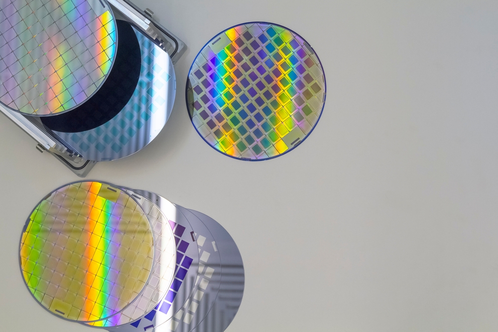
Single-wafer systems for surface preparation processes leverage JST’s wet bench expertise to create comprehensive wet processing portfolio.
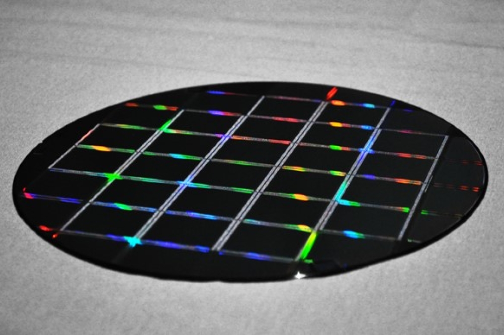
JST Manufacturing has formally introduced its Ospray family of single-wafer wet processing systems. In production at multiple customer sites, the Ospray tools leverage JST’s extensive expertise in wet chemistries, positioning the company to become a complete supplier of wet processing solutions. Key target markets for Ospray include MEMS and sensors, analog and communications chips, and, especially, compound semiconductors (CS) used in optoelectronics applications such as lasers, LEDs and photodiodes.
According to data published by market research firm Yole Group, the market for CS substrates is predicted to reach $2.3 billion by 2027, growing at a compound annual rate of 17% between 2021 and 2027. Materials primarily driving this growth are silicon carbide (SiC), indium phosphide (InP) and gallium nitride (GaN). These complex yet fragile substrates require high-precision, high-uniformity surface preparation, making them ideally suited for the Ospray single-wafer tools.
“JST has established a strong position in the batch immersion space over more than four decades. With the rise of compound semiconductors and other materials being processed in smaller volumes on 200mm wafers, we saw a gap in the market for an automated single-wafer system that could meet these customers’ needs,” said Ryan Zrno, JST Manufacturing’s chief executive officer. “With Ospray in our arsenal, using the same chemistries as our bench systems, we can lay out all the options for customers to determine their optimal wet processing approach. Moreover, by serving as a single source for wet processing solutions, we help customers streamline their supply chain.”
The small-footprint, highly reliable Ospray systems include the Ospray SP front-end tool for critical etch and cleaning processes and Ospray MLO for back-end metal liftoff and photoresist strip processes. Delivering superior uniformity and repeatability – from 3% to <1% depending on the process – Ospray can be configured with up to eight chambers, and its vertical integration enables high flexibility in module design and tank implementation.
“Our customers who’ve purchased Ospray are sharing excellent early results,” noted Brian Thomas, director of sales for JST. “For example, customers are realizing uniformity and repeatability advantages over batch and other single-wafer systems for etching and cleaning complex InP substrates. Multiple customers are also seeing Ospray’s benefits for automated processing on wafers larger than 200mm. We already have orders in hand for 300mm Ospray systems, which we will be building and shipping in 2024.”
Designed with an internal stainless steel system isolated from process chemistries, Ospray single-wafer systems are fully programmable, from wafer rotation speed, chemical flow rate and pressure control, to the servo-controlled oscillating spray nozzles and implementation of chemistries, which can be used in a single pass or recirculated. Chemistry handling is carefully managed, from delivery to post-process disposal, with customized recipes enabling diversion of waste streams to designated drains, in alignment with customers’ sustainability efforts.
For U.S.-based customers, adding Ospray to its wet processing family further positions JST to benefit from heightened focus on domestic growth and onshoring in the U.S. semiconductor industry. Regardless of region, Ospray customers receiving unlimited training from JST engineers during the startup phase and 24/7 customer service for the life of the system, not merely during the warranty period.


