Photonic pursues silicon-based approach to Quantum Computing
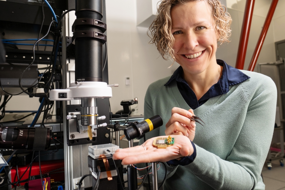
Photonic Inc., a company building one of the world’s first scalable, fault-tolerant, and unified quantum computing and networking platforms based on photonically linked silicon spin qubits, has introduced its quantum architecture.
Photonic’s unique approach to quantum computing stands to accelerate innovation across the quantum ecosystem.
“Quantum computing is real, and we believe that—within five years, significantly sooner than the widely accepted timeframe—we will be the first quantum computing company to offer a scalable, distributed, and fault-tolerant solution,” said Dr. Stephanie Simmons, Founder and Chief Quantum Officer of Photonic and Co-chair of Canada’s National Quantum Strategy Advisory Board. “These are the capabilities that must be delivered for quantum computing to be a relied upon across industries, and we believe that we have correctly identified the silicon T centre as the missing component needed to finally unlock the first credible path to impactful commercial quantum computing.”
Photonic specializes in spin-photon interfaces in silicon, silicon integrated photonics, and quantum optics. Photonic has committed to silicon—the chemical element serving as the backbone of modern telecommunications and computation—as the dominant enabling design in quantum computing.
To become universally accessible and useful, quantum computing must be able to:
• achieve large numbers of identical, manufacturable, high-quality qubits
• operate under diverse environmental conditions
• communicate rapidly and reliably among those qubits over networks
Leveraging colour centers and telecom photons, Photonic's patented technology provides computing (with spin qubits), networking (via photons), and memory. Photonic links in silicon deliver quantum entanglement not only between qubits on the same chip but also among multiple quantum chips. Silicon-based qubits enjoy substantially greater microelectronic-style scalability than other types of qubits. Indeed, Photonic’s architecture achieves horizontal scaling. Photonic's highly connected qubit architecture also enables use of efficient quantum error correction codes, such as quantum LDPC (Low Density Parity Check) codes. These codes are known for extremely low physical to logical qubit overheads and fast and efficient hardware implementation.
Such attributes will prove increasingly crucial as quantum computing drives more applications. For example, Photonic’s technology can deliver unparalleled security to global digital communications, offering a solution to the cybersecurity threat posed by the development of quantum computing. Beyond internet cybersecurity, quantum computing promises transformative capabilities for modelling and simulation of complex systems and processes in areas such as climate modelling, materials development, and creation of life-saving pharmaceuticals.
“Ultimately, the breadth of problems to which quantum computing can offer a solution means it will have a tangible, meaningful impact on people all around the world,” said Dr. Paul Terry, Photonic Chief Executive Officer. “We’re moving to large-scale, accessible quantum computers networked together to provide access to quantum services that will enable companies and governments to suddenly tackle problems that are, right now, beyond our capabilities because of the inescapable constraints of classical computing. It’s incredibly thrilling to be on the cusp of this inflection point in quantum computing and, more broadly, physics history.”
Photonic, which has built one of the world’s largest teams of quantum silicon experts, has raised a total of $140 million USD in funding to date, and benefits from leveraging the globally mature manufacturing ecosystem for semiconductors and telecoms. The company is led by innovators with deep expertise in delivering disruptive technologies.
Dr. Simmons is a Tier 2 Canada research chair in silicon quantum technologies and a Canadian Institute for Advanced Research fellow in quantum information science. She is an associate professor in the physics department at Simon Fraser University in Burnaby, British Columbia, who has twice been accorded a Physics World Top 10 Breakthrough of the Year (2013 and 2015) for her work in silicon quantum technologies.
Dr. Terry is a seasoned executive, entrepreneur, engineer, and angel investor who has founded or has been one of the founding employees at six successful companies in areas from big data systems to supercomputing, to IP services and telecom networking.
In related news, Photonic also announced today Photonic Collaborating with Microsoft to Power Global Quantum Ecosystem, and Photonic Raises $100 Million USD for Quantum Technology from BCI, Microsoft, and Other Investors. In addition, a Photonic technical paper, Scalable Fault-Tolerant Quantum Technologies with Silicon Colour Centres, details the company’s novel architecture, and a Microsoft blog post, Microsoft and Photonic join forces on the path to quantum at scale, offers more perspective on that company’s collaboration with Photonic. offers more perspective on that company’s collaboration with Photonic.


