Cadence EMX 3D Planar Solver certified for Samsung Foundry
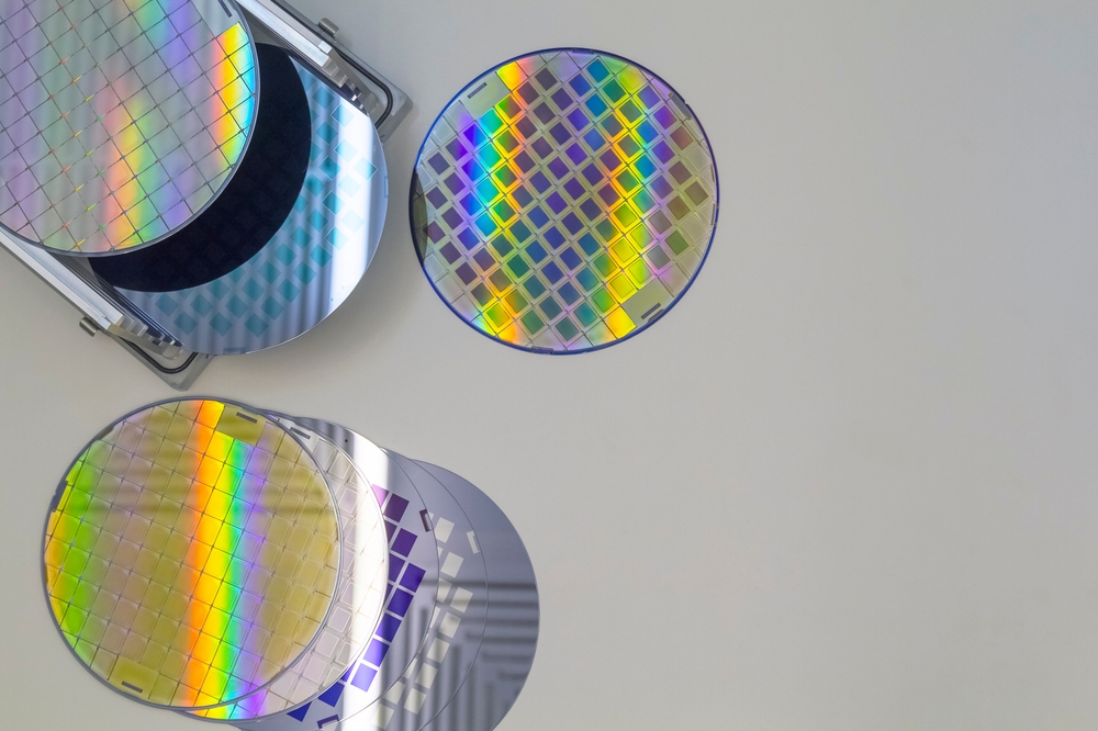
EMX 3D Planar Solver empowers customers to achieve accurate, high-capacity EM analysis, resulting in first-pass silicon success and faster time to market.
Cadence Design Systems says that the Cadence® EMX® 3D Planar Solver is now certified for use with Samsung Foundry’s advanced 8nm Low Power Plus (LPP) process technology. The EMX Solver is said to be the first electromagnetic (EM) solver on the market to achieve this milestone, having successfully passed all of Samsung’s detailed certification criteria. Joint customers can confidently adopt the EMX Solver into their advanced designs to ensure highly accurate, high-capacity EM analysis, avoiding unintentional parasitics and crosstalk effects. Through this latest collaboration between Cadence and Samsung Foundry, customers can achieve first-pass silicon success and accelerate time to market.
A foundry-certified EM modeling engine is essential for successful block- and chip-level analysis and signoff. Accurate EM models are fundamental for designing ICs for today’s cutting-edge applications. A wide array of inductors featuring various configurations were manufactured and measured by Samsung for the certification process, and the EMX Solver performed with extremely high accuracy in all categories.
With the EMX Solver, customers can simulate large circuit blocks, characterize the EM behavior of passive components, and analyze on-chip parasitics. The solver can analyze advanced-node process fabrication effects, including width- and spacing-dependent effects. The EMX Solver is seamlessly integrated in Cadence’s custom/analog design flow with all Virtuoso® releases, including the AI-based Virtuoso Studio, as well as the Virtuoso Analog Design Environment and Spectre® RF Option.
“Through our longstanding collaboration with Cadence, we’ve provided customers with the powerful tools they need to achieve first-pass silicon success with advanced node designs,” said Sangyun Kim, vice president and head of the Foundry Design Technology Team at Samsung Electronics. “Our strong partnership ensures that customers can leverage the EMX 3D Planar Solver to accelerate design closure with our 8nm LPP process technology.”
“Today’s designs at advanced process nodes must withstand crosstalk effects,” said Ben Gu, corporate vice president of R&D for the Multiphysics System Analysis Business Unit at Cadence. “Accurate, high-capacity EM analysis is essential to safeguard these designs from unintentional parasitics. The Cadence EMX 3D Planar Solver is not only the industry’s gold-standard EM, it now boasts Samsung certification so that our mutual customers can continue designing at the very edge of the technology, confidently.”
The EMX 3D Planar Solver supports the Cadence Intelligent System Design™ strategy, enabling system-on-chip (SoC) design excellence and system innovation. For more information on the EMX 3D Planar Solver, please visit www.cadence.com/go/EMXSolverCertification.


