Imec grants public access to virtual fab
Beyond the ICT industry, imec aims to guide academics and policy makers with actionable data.
Imec has launched a freely accessible version of its imec.netzero virtual fab. The tool offers a quantified view of the environmental impact of IC manufacturing, providing valuable insights for academics, policy makers and designers. With the release of this free web application, imec aims to support industry in reducing its environmental impact, beyond the semiconductor supply chain.
Semiconductor manufacturing is a complex process with diverse environmental implications; from high energy consumption to usage of scarce materials and greenhouse gas emissions. With the growth of its market and the Paris agreement targets on climate change in mind, the industry is aiming to optimize process flows. However, to determine and mitigate processes or technologies with high environmental impact, a wealth of data is needed. This is tackled within imec’s Sustainable Semiconductor Technologies and Systems (SSTS) research program, a collaborative framework involving the entire semiconductor ecosystem; from end users of electronics to fabs, foundries, material, and equipment manufacturers, working together with academia and governments.
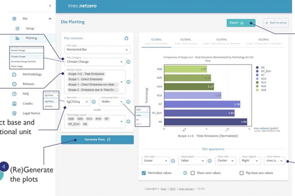
To accurately quantify the environmental impact of Integrated Circuit (IC) manufacturing, imec has developed a virtual fab called imec.netzero. This web application utilizes data from its own fab, which is continuously benchmarked with data from equipment, material and fab partners such as Air Liquide, Applied Materials, ASM, ASML, Edwards, Kurita, Lam Research, SCREEN, Tokyo Electron, GlobalFoundries, Samsung Electronics and TSMC. The virtual fab follows the Life-Cycle Assessment methodology and collects and analyzes data on the energy, materials, chemicals, gases, and other resources used in each process step of making an IC. Partners can access a private imec.netzero software application, that provides a detailed analysis to quantify embodied emissions and other environmental impacts about current and future IC technologies, providing tangible actions. Through its now , imec aims to reach a much broader audience. The public version offers access to the same fab models and process databases as imec.netzero Private. Whilst more limited (e.g., restricted to current technologies and Scope 1+2 from the Greenhouse Gas Protocol) this webapp provides unique insights into data otherwise not accessible to the public. For example, visual presentations of climate change (CO2 emissions), electrical energy consumption or total water usage can be generated for multiple logic and memory technologies (from N28 onwards), based on fabrication in diverse geographical locations.
“Our aim is to offer transparent and high-quality data on the environmental impact of IC manufacturing, beyond the semiconductor supply chain and our SSTS program”, explains Cédric Rolin, program manager at imec. “Surpassing current available literature, our tool provides value to product designers, environmental researchers, and policymakers seeking industry impact data.”.


