
Applied Materials and CEA-Leti unveil Joint Lab
Applied Materials, Inc. and CEA-Leti are expanding their longstanding collaboration to focus on developing differentiated materials engineering solutions for several specialty semiconductor applications.
The joint lab, which represents CEA-Leti’s highest level of collaboration, aims to accelerate device innovations for Applied’s customers serving ICAPS markets (IoT, Communications, Automotive, Power and Sensors). Technology applications in those fields include photonics, image sensors, RF communications components, power devices and heterogeneous integration.
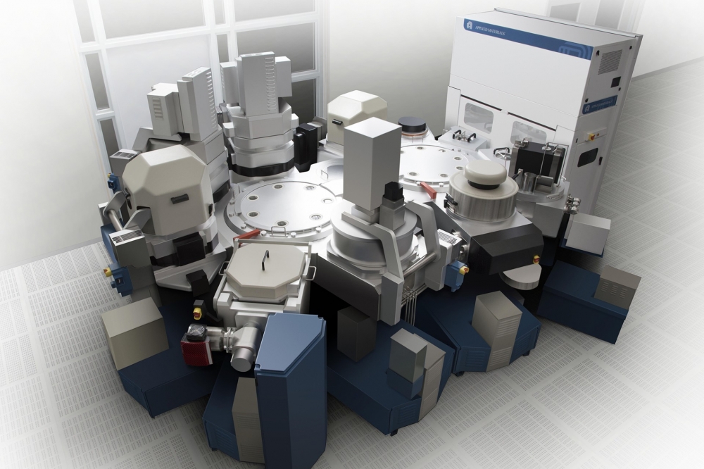
Demand for ICAPS applications and devices is being driven by industrial automation, the Internet of Things (IoT), electric vehicles, green energy and smart grid infrastructure, among other major high growth markets. Projects at the joint lab will focus on developing solutions for a variety of materials engineering challenges to enable the next wave of ICAPS device innovation. The joint lab features several of Applied Materials’ 200mm and 300mm wafer processing systems and leverages CEA-Leti’s world-class capabilities for evaluating performance of new materials and device validation. Improvements in power consumption, performance and area/cost, along with faster time to market (PPACt™), will be key objectives of the joint team.
“CEA-Leti and Applied Materials aim to accelerate innovation and advance the roadmaps of a wide range of specialty semiconductor technologies,” said Aninda Moitra, corporate vice president and general manager of Applied Materials’ ICAPS business. “Our work at the joint lab builds upon more than a decade of successful collaboration and further strengthens our combined ability to enable faster time to innovation for ICAPS chipmakers.”
“For the past 10 years, Applied Materials and CEA-Leti have collaborated through multiple, specific joint development programs, which have set the stage for establishing our new joint lab,” said Sébastian Dauvé, the institute’s CEO. “Past projects included work in domains such as advanced metrology, materials for memory applications and optical devices, bonding techniques, materials deposition and film growth (PVD, CVD, ECD, Epitaxy) and chemical-mechanical planarization (CMP). Our results brought high value to both partners and to customers around the world, and we look forward to expanding our engagement with this new lab.”
“The joint lab, which is based at CEA-Leti, will host Applied Materials scientists and involve some of its latest-generation equipment,” Dauvé said. “In addition to developing differentiated technological solutions for Applied’s customers, the work performed at the joint lab will help overcome current technical hurdles in support of CEA-Leti’s internal R&D programs.”


