Purdue honours Boilermaker and innovative visionary in semiconductors

Engineering alumnus’ discovery laid the foundation for advanced packaging, system integration research.
Purdue University will recognize the impact of alumnus and semiconductor pioneer John Atalla with the naming of the newest system integration and packaging research institute on campus.
The Atalla Institute for Advanced System Integration and Packaging (ASIP) will honor Purdue graduate Martin (John) M. Atalla, known as the co-inventor of the silicon MOSFET (metal-oxide-semiconductor field-effect transistor), one of the most widely used types of integrated circuits in microchips. With an estimated 10^22 silicon MOSFETs made so far and many more to come, it is the most manufactured invention in history. Atalla’s work led to the chips that make many aspects of daily life possible today.
“The work of Atalla and his team at Bell Labs led to the demonstration of the first silicon MOSFET in 1959 and blazed the trail for modern integrated circuit chips,” said Mark Lundstrom, Purdue’s chief semiconductor officer. “Our students and faculty can now honor his name by continuing to further his work.”
Atalla studied mechanical engineering at Purdue, receiving a master’s degree in 1947 and a doctorate in 1949. He was honored as a Purdue Distinguished Engineering Alumnus in 2002.
Purdue’s Institute for Advanced System Integration and Packaging was announced in October during the university’s Semiconductor Week. Bringing together four on-campus research centers, the institute builds on Purdue’s established research in advanced packaging and system integration and puts new focus on advanced electronic systems in packages, which are widely expected to drive progress in electronic systems in the decades to come.
After Purdue, Atalla began investigating the surface properties of silicon semiconductors at Bell Laboratories. His work led to the emergence of the silicon MOSFET in 1960. The next year, Atalla joined Hewlett-Packard and became the first manager of HP’s Semiconductor Lab. In 1969 he joined Fairchild Camera and Instrument Corp.
The Atalla Corp. was founded in 1972 to address security problems in banking. In 1990 Atalla retired, renowned as the inventor of the PIN, or personal identification number, and the Atalla Box, which at one point secured 80% of all ATM transactions worldwide. Atalla returned to work in 1993, focusing on encryption technology for the internet, and founded TriStrata Corp. in 1996.
He was a native of Port Said, Egypt, and died in 2009 at age 85.
ASIP hosted its first international workshop recently, with industry and academic leaders in attendance to address the challenges to research, “lab-to-fab” translation and workforce necessary to build future microelectronic systems. The workshop was hosted in partnership with the Applied Research Institute, host of the Silicon Crossroads Microelectronics Commons Hub; imec USA; Cadence; and Osaka University.
The need for microchips in areas from computing, mobile communications and vehicles to defense and biological applications requires future advanced system integration and packaging like that represented by Purdue’s research.
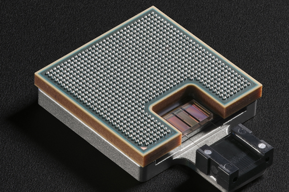
Chip packaging ensures the functionality and reliability of a system, as multiple chips are connected electrically. Advanced packaging aims to revolutionize packaging by enabling complex functionality while reducing cost.
Purdue is a national leader in microelectronics materials, devices, chip design, tool development, manufacturing, packaging and sustainability, spanning the semiconductor ecosystem in software and hardware with long-standing faculty excellence.
Strategic initiatives in semiconductors, such as the first comprehensive Semiconductor Degrees Program, which was announced before the CHIPS and Science Act passed in 2022, are intended to prepare a next-generation workforce for industry. Economic development and research collaboration is underway, including with Skywater, MediaTek and Belgium-based imec.
As part of the Purdue Computes initiative, Purdue’s growing semiconductor innovation ecosystem includes $49 million in new facilities and tools for the Birck Nanotechnology Center, which will also be accessible by Ivy Tech Community College, Indiana’s statewide community college and a local partner with Purdue in developing next-level workforce and brain gain strategies for Indiana.
The Indiana-led proposal “Silicon Crossroads” was announced Sept. 20 by the U.S. Department of Defense as one of eight Microelectronics Commons Hubs selected out of over 80 proposals across the country. The Naval Surface Warfare Center, Crane Division (NSWC Crane), in Indiana will manage the program. Purdue will collaborate with many consortium members in the coming years.
Purdue announced in September the creation of Purdue@Crane, a permanent Purdue presence for national security research collaboration with NSWC Crane, including participation in the WestGate Foundry with companies such as Everspin Technologies and NHanced Semiconductors.


