
EV Group brings layer transfer technology yo high volume manufacturing
Infrared laser cleave technology enables ultra-thin-layer transfer from silicon substrates with nanometer precision, revolutionizing 3D integration for advanced packaging and transistor scaling.
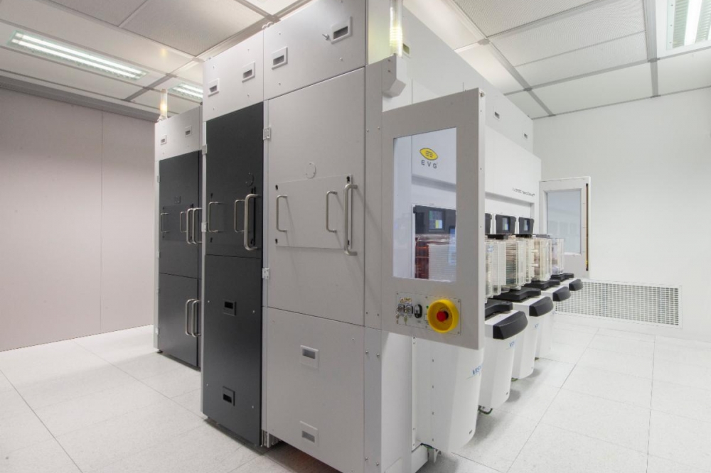
EV Group has introduced the EVG®850 NanoCleave™ layer release system—the first product platform to feature EVG’s revolutionary NanoCleave technology. The EVG850 NanoCleave system enables nanometer-precision release of bonded, deposited or grown layers from silicon carrier substrates using an infrared (IR) laser coupled with specially formulated inorganic release materials in a proven, high-volume-manufacturing (HVM) capable platform. As a result, the EVG850 NanoCleave eliminates the need for glass carriers—enabling ultra-thin chiplet stacking for advanced packaging, as well as ultra-thin 3D layer stacking for front-end processing, including advanced logic, memory and power device formation, to support future 3D integration roadmaps.
The first EVG850 NanoCleave systems have already been installed at customer facilities, and nearly two dozen product demonstrations are underway with customers and partners at customer sites and EVG’s headquarters.
Silicon Carriers Benefit 3D Stacking and Back-end Processing
In 3D integration, glass substrates have become an established method for building up device layers through temporary bonding with organic adhesives, using an ultraviolet (UV) wavelength laser to dissolve the adhesives and release the device layers, which are subsequently permanently bonded onto the final product wafer. However, glass substrates are difficult to process with semiconductor fab equipment that have been designed primarily around silicon, and that require costly upgrades to enable glass substrate processing. In addition, organic adhesives are generally limited to processing temperatures below 300 °C, limiting their use to back-end processing.
Enabling silicon carriers with inorganic release layers avoids these temperature and glass carrier compatibility issues. In addition, the nanometer precision of IR laser-initiated cleaving allows for processing extremely thin device wafers without changing processes of record. Subsequent stacking of such thin device layers enables higher-bandwidth interconnects and new opportunities to design and segment dies for next-generation, high-performance devices.
Next-generation Transistor Nodes Require Thin-layer Transfer Processes
At the same time, transistor roadmaps for the sub-3-nm node call for new architectures and design innovations such as buried power rails, backside power delivery networks, complementary field-effect transistors (CFETs) and 2D atomic channels, all of which require layer transfer of extremely thin materials. Silicon carriers and inorganic release layers support process cleanliness, material compatibility and high processing temperature requirements for front-end manufacturing flows. However, until now, silicon carriers had to be completely removed using grinding, polishing and etching processes, which results in micron-range variations across the surface of the working device layer, making this method unsuitable for thin-layer stacking at advanced nodes.
“Releasable” Fusion Bonding
The EVG850 NanoCleave utilizes an IR laser and inorganic release materials to enable laser cleaving from silicon carriers with nanometer precision in production environments. The innovative process eliminates the need for glass substrates and organic adhesives, enabling front-end process compatibility for ultra-thin-layer transfer and downstream processes. The most demanding front-end processing is supported by the EVG850 NanoCleave’s high-temperature compatibility (up to 1000 °C) while the room-temperature IR cleaving step ensures device layer and carrier substrate integrity. The layer transfer process also eliminates the need for expensive solvents associated with carrier wafer grinding, polishing and etching.
The EVG850 NanoCleave is based on the same platform as EVG’s industry-leading EVG850 series of automated temporary bonding/debonding and silicon-on-insulator (SOI) bonding systems, with a compact design and HVM-proven wafer handling system.
According to Dr. Bernd Thallner, corporate R&D project manager at EV Group, “Since EVG’s founding more than 40 years ago, our vision has been steadfast in being the first in exploring new techniques and serving next-generation applications of micro- and nanofabrication technologies. Recently, 3D and heterogeneous integration have stepped into the spotlight as key drivers of performance improvements on new semiconductor device generations. This in turn has brought wafer bonding front and center as a critical process for continuing PPACt (power, performance, area, cost and time-to-market) scaling. With our new EVG850 NanoCleave system, EVG has merged the benefits of temporary bonding and fusion bonding into one versatile platform supporting our customers’ ability to extend their future roadmaps in both advanced packaging and next-generation scaled transistor design and manufacturing.”


