
DNP develops photomask process for 3nm EUV lithography
Responding to semiconductor market needs where circuit line widths are becoming increasingly finer.
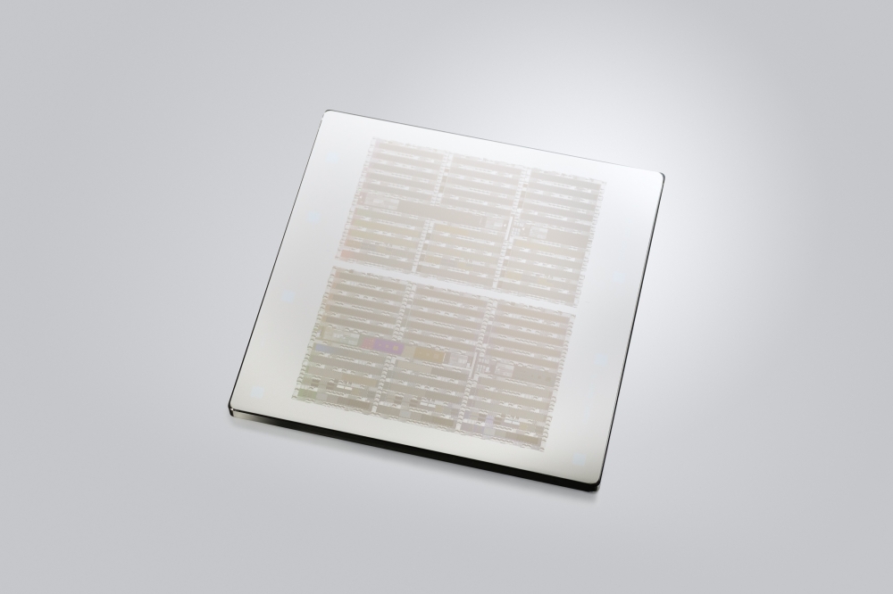
Dai Nippon Printing Co., Ltd. (DNP) has successfully developed a photomask manufacturing process capable of accommodating the 3-nanometer (10-9 meter) lithography process that supports Extreme Ultra-Violet (EUV) lithography, the cutting-edge process for semiconductor manufacturing.
In doing so, the company is responding to the need for ever finer circuit line widths in line with the shift to high-performance in the logic semiconductors used in smartphones and data centers.
EUV lithography technology using EUV light sources has recently become established, and the production of cutting-edge logic semiconductors using EUV lithography is forging ahead. Going forward, the miniaturization of semiconductor circuit line widths is expected to make further progress, including the supply of products using 3nm logic semiconductors in 2023. At the same time, EUV lithography is increasingly being adopted in memory semiconductors, and EUV compatibility has become indispensable in the supply of cutting-edge semiconductors.
DNP has continually responded to the demands of semiconductor manufacturers in terms of performance and quality. In 2016, the company became the world's first merchant photomask manufacturer to introduce the multi-beam mask writing tool (MBMW)1. In 2020 it developed a photomask manufacturing process for 5nm EUV lithography processes2, and have been supplying masks that meet the needs of the semiconductor market. In this latest development, in order to meet the needs of further miniaturization, DNP has developed a photomask for EUV lithography capable of supporting 3nm processes.
MBMW introduced by DNP in 2016 is capable of irradiating with approximately 260,000 electron beams, and can significantly shorten the lithography time even with complex pattern shapes. On this occasion, we have improved the manufacturing process by leveraging the characteristics of the equipment, while optimizing the data correction technology and processing conditions to match the complex curved pattern structure of photomask for EUV lithography.
DNP has installed a new MBMW, and plans to commence operations in the second half of 2024. We will also strengthen our support for semiconductor manufacturing in advanced areas such as photomasks for EUV lithography.
DNP will promote joint development of EUV photomasks for next-generation EUV exposure equipment with imec, a cutting-edge international research organization headquartered in Belgium.
DNP will provide the newly developed photomask capable of supporting 3nm EUV lithography to semiconductor manufacturers throughout the world, as well as semiconductor development consortiums, manufacturing equipment makers and material manufacturers. In addition, we will also support the development of peripheral technologies for EUV lithography, aiming for annual sales of 10 billion yen in 2030.
Through joint development with partners, such as imec, DNP will continue to develop more advanced photomasks capable of supporting processes finer than 3nm and even beyond 2nm.


