CEA-Leti reports 'breakthrough' 3D Sequential Integration (3DSI)

Achievement establishes the feasibility of manufacturing high-performance silicon CMOS devices above an industrial platform, including state-of-the-art BEOL, without compromising the performance of the bottom layer.
CEA-Leti at IEDM 2023 described the world’s-first 3D sequential integration (3DSI) of CMOS over CMOS with advanced metal line levels, which brings 3DSI with intermediate BEOL closer to commercialization.
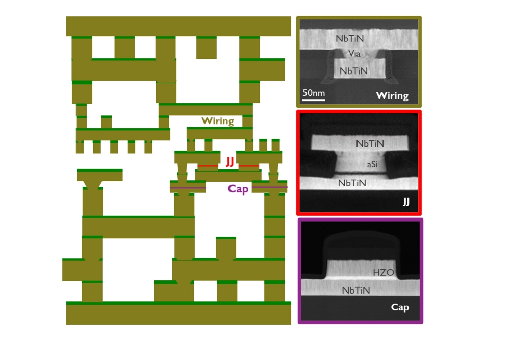
This breakthrough, detailed in the paper “3D Sequential Integration with Si CMOS Stacked on 28nm Industrial FDSOI with Cu-ULK iBEOL Featuring RO and HDR Pixel”, stems from the demonstration of a monocrystalline CMOS stacked sequentially above an industrial CMOS platform (28nm FDSOI) and four metal levels. The top CMOS device process was carried out at 500°C in a FEOL 300mm fabrication above state-of-the art CU/ULK 28nm BEOL.
“This achievement establishes the feasibility of manufacturing high-performance silicon CMOS devices above an industrial platform, including state-of-the-art BEOL, without compromising the performance of the bottom layer. It allows reaching the full potential of 3DSI with top devices having high performance, low variability and CMOS co-integrability in contrast with BEOL transistors,” said Perrine Batude, a co-author of the paper and leader of 3DSI integration in CEA-Leti.
Full 3DSI, in which monocrystalline CMOS devices are stacked above an industrial CMOS process, specifically when it integrates an intermediate BEOL (iBEOL) with Cu and ULK, previously has eluded researchers. “This work aims to demonstrate such integration, provide methodologies to achieve it, and analyze the performance of 3D circuits,” the paper explains.
Batude said this R&D also is a world's-first 3DSI demonstration of such scale, featuring functional 3D circuit demonstrations, such as 3D ring oscillators and a single-exposure high-dynamic-range, two-layer pixel.
Additionally, the inclusion of the polysilicon ground plane “is anticipated to ensure a remarkable 40dB isolation up to 100GHz, showing a relevance of this integration for RF applications,” she said.
The paper provides a comprehensive showcase of a 3DSI platform, featuring functional 3D circuit demonstrations such as 3D inverters, 3D ring oscillators and a single-exposure high dynamic range two-layer pixel.


