+44 (0)24 7671 8970
More publications     •     Advertise with us     •     Contact us
 
Loading...
News Article

CEA-Leti develops 'cost-saving' CMOS-compatible 200mm process technology

News

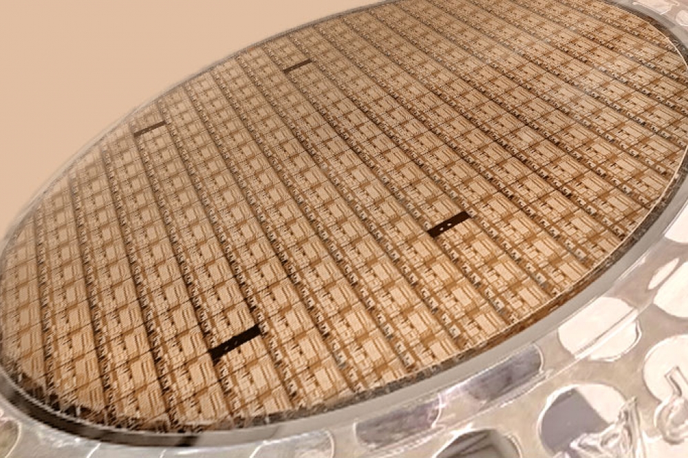
CEA-Leti has developed a 200mm gallium nitride/silicon (GaN/Si) process technology compatible with CMOS cleanrooms that preserves the high performance of the semiconductor material and costs less than existing GaN/SiC technology.

In one of nine presentations at IEDM 2023, the institute said that current GaN high-electron-mobility-transistor (HEMT) technologies used in telecom or radar applications come on small GaN/SiC substrates and require processing in dedicated cleanrooms.

The high-performance SiC substrates used to grow GaN layers are very expensive and available only in relatively small size. This R&D project developed GaN/silicon technology (GaN/Si) on 200mm and later for 300mm wafer diameters in CMOS-compatible cleanrooms to reduce substrate cost and benefit from existing high-performance cleanroom facilities.

As a result, CEA-Leti’s GaN/Si technology performance at 28 GHz is gaining ground on GaN/SiC technology in terms of power density.

“Our goal was to reach existing state-of-the-art GaN HEMT performance at ~30 GHz with a 200mm CMOS- compatible GaN/Si technology and to compete with GaN/SiC technology,” said Erwan Morvan, CEA-Leti scientist and lead author of the paper, "6.6W/mm 200mm CMOS Compatible AlN/GaN/Si MIS-HEMT with In-Situ SiN Gate Dielectric and Low Temperature Ohmic Contacts”.

“This work demonstrates that CMOS-compatible 200mm SiN/AlN/GaN MIS-HEMT on silicon technology is a promising candidate for applications like 5G/6G infrastructure, satcom, radar for UAV detection or earth observation. It should enable less expensive devices while keeping high power density, high efficiency, light weight and compactness,” he said.

The devices developed in this work, which are designed for RF amplifiers and switches, can be used in those applications around 30 GHz.

While reliability testing on the process technology is just beginning, CEA-Leti’s ongoing R&D in this area will include increasing the raw output power and efficiency of its MIS-HEMT transistors, integrating its improved process modules to boost device performance & increase operation frequency toward 100+ GHz, and 3D integration of GaN/Si chips on 300mm Si wafers.

Reality AI Explorer Tier offers free AI/ML development access
AEM introduces new generation of Automated Burn-In Systems
NPUs are emerging as the main rival to Nvidia’s AI dominance, says DAI Magister
Camtek receives a $20M order from a Tier-1 OSAT
Free samples of every STMicroelectronics NPI IC available from Anglia
NY CREATES and SEMI sign MoU
Major government investment to 'propel' Canada
QuickLogic announces $5.26 million contract award
ASNA and Athinia collaborate
Global sales forecast to reach record $109 billion in 2024
AMD to acquire Silo AI
Nanotronics unveils 'groundbreaking' Gen V AI Model
Aitomatic unveils SemiKong
Biden-Harris Administration reveals first CHIPS for America R&D facilities and selection processes
Collaboration to produce cutting-edge AI accelerator chips
Oxford Ionics breaks global quantum performance records
Adeia wins ECTC Award for paper on “Fine Pitch Die-to-Wafer Hybrid Bonding”
AEM introduces new generation of Automated Burn-In Systems
Sydney council forges vital semiconductor agreement
EV Group's EVG880 LayerRelease wins 2024 Best of West
Biden-Harris Administration to invest up to $1.6 billion
Cyient sets up subsidiary for semiconductor business
EMD Electronics network leaders honoured
Accenture acquires Cientra
Introducing Park FX200
Deep learning chipset market to surge to $72.8 billion by 2033
PI Innovation Award 2024: Nanobodies for Diagnostic and Therapeutic Applications
Graphcore joins Softbank Group
Kaman Measuring highlights high precision displacement sensors
Si2 reveals recipients of Annual Power of Partnerships Award
Advantest achieves ASPICE Level 2 Certification for V93000 SmarTest 8 Software
Semiconductors to become a trillion-dollar industry by 2030
×
Search the news archive

To close this popup you can press escape or click the close icon.
Logo
×
  • 1st January 1970
  • 1st January 1970
  • 1st January 1970
  • 1st January 1970
  • 1st January 1970
  • 1st January 1970
  • 1st January 1970
  • 1st January 1970
  • View all news 22645 more articles
Logo
×
Register - Step 1

You may choose to subscribe to the Silicon Semiconductor Magazine, the Silicon Semiconductor Newsletter, or both. You may also request additional information if required, before submitting your application.


Please subscribe me to:


You chose the industry type of "Other"

Please enter the industry that you work in: