+44 (0)24 7671 8970
More publications     •     Advertise with us     •     Contact us
 
Loading...
News Article

Earthquake temporarily halts Japan facilities

News


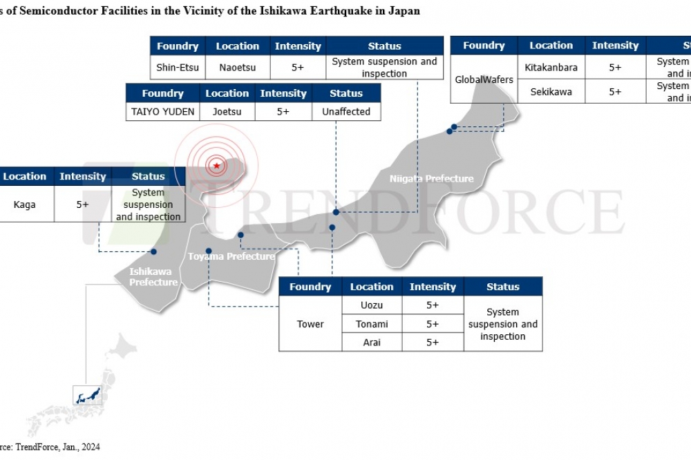
TrendForce’s investigation into the impact of the recent strong earthquake in the Noto region of Ishikawa Prefecture, Japan, reveals that several key semiconductor-related facilities are located within the affected area.

This includes MLCC manufacturer TAIYO YUDEN, silicon wafer (raw wafer) producers Shin-Etsu and GlobalWafers, and fabs such as Toshiba and TPSCo (a joint venture between Tower and Nuvoton).

Given the current downturn in the semiconductor industry and the off-peak season, along with existing component inventories and the fact that most factories are located in areas with seismic intensities of level 4 to 5—within the structural tolerance of these plants—preliminary inspections indicate no significant damage to the machinery, suggesting the impact is manageable.

In terms of silicon wafer production, Shin-Etsu and GlobalWafers' facilities in Niigata are currently shut down for inspection. The crystal growth process in raw wafer manufacturing is particularly sensitive to seismic activity. However, most of Shin-Etsu's crystal growth operations are primarily in the Fukushima area, thus experiencing limited impact from this earthquake. SUMCO reported no effects.

On the semiconductor front, Toshiba's Kaga facility in the southwestern part of Ishikawa Prefecture is currently undergoing inspections. This site includes a six-inch and an eight-inch factory, along with a twelve-inch facility slated for completion in the 1H24. Additionally, the three TPSCo factories in Uozu, Tonami, and Arai—co-owned by Tower and Nuvoton (formerly Panasonic)—are all undergoing shutdowns for inspections. In contrast, USJC (UMC's acquisition of the Mie Fujitsu plant area in 2019) was not affected.

MLCC manufacturer TAIYO YUDEN’s new Niigata plant, designed to withstand seismic activity up to level 7, reported no equipment damage. Murata (MLCC fabs only) and TDK’s MLCC plants experienced seismic intensities below level 4 and were not notably affected. However, Murata’s other factories (Non-Production MLCC) in Komatsu, Kanazawa, and Toyoma, which are in the areas with seismic intensity above 5, were closed for the New Year holiday, and staff are currently assessing any damage.

Tektronix and EA Elektro-Automatik offer expanded power portfolio
83% of supply chains can’t respond to disruptions in 24 hours
CMC Microsystems and ventureLAB sign MoU
Renesas introduces FemtoClock 3 timing solution
Mycronic receives order for SLX mask writer
Rapidus reveals US subsidiary and opens Silicon Valley office
Infineon introduces news MOTIX motor gate driver IC
Brewer Science unveils Smart Warehouse Monitor System
Symposium to showcase breakthroughs in microelectronics
CHIPS for America promotes over $50 million funding opportunity
SEMI University launches in-person courses
Samsung Electronics to establish Texan semiconductor ecosystem
Semiconductor chips drive innovation in AI and industries
Semiconductor equipment sales slip to $106.3 billion
Mouser Electronics receives 2023 Global Best Service Distributor of the Year Award from Diodes Incorporated
Quantum processor testing and measurement facilities up and running
Semiconductor Research Corporation announces 2024 call for research
Trend report unveils the future of circular electronics
PCIM Europe 2024: highlights and new records
PI contributes to technology node development
QP Technologies achieves ANSI/ESD S20.20 Certification
Renesas commences operations of Kofu Factory
TRI wins three Innovation Awards
Tektronix and recently acquired EA Elektro-Automatik offer expanded power portfolio
NEDO approves Rapidus’ FY2024 Plan and Budget
SK hynix signs Advanced Chip Packaging agreement
Renesas expands Quick Connect Studio
Infineon and Amkor deepen partnership
AP&S establishes site in the USA
Dracula Technologies selected by STMicroelectronics
RAIN RFID data to transform corporate sustainability initiatives
Integrated AMR replaces reed switches and hall effect sensors
×
Search the news archive

To close this popup you can press escape or click the close icon.
Logo
×
  • 1st January 1970
  • 1st January 1970
  • 1st January 1970
  • 1st January 1970
  • 1st January 1970
  • 1st January 1970
  • 1st January 1970
  • 1st January 1970
  • View all news 22645 more articles
Logo
×
Register - Step 1

You may choose to subscribe to the Silicon Semiconductor Magazine, the Silicon Semiconductor Newsletter, or both. You may also request additional information if required, before submitting your application.


Please subscribe me to:


You chose the industry type of "Other"

Please enter the industry that you work in: