Loading...
News Article

Electron-beam lithography system for Dresden fab

News

Investment in new production tool for the semiconductor equipment industry.

Jenoptik is investing a low double-digit million-euro amount in a state-of-the-art system for the high-tech fab currently under construction in Dresden. The new electron-beam lithography system (E-Beam) will be used to manufacture high-precision micro-optical components for customers in the semiconductor and optical communication sectors. The manufacturer is the Jena based e-beam technology specialist Vistec Electron Beam GmbH. The system will be delivered at the beginning of 2025.

Creating the smallest structures with maximum precision

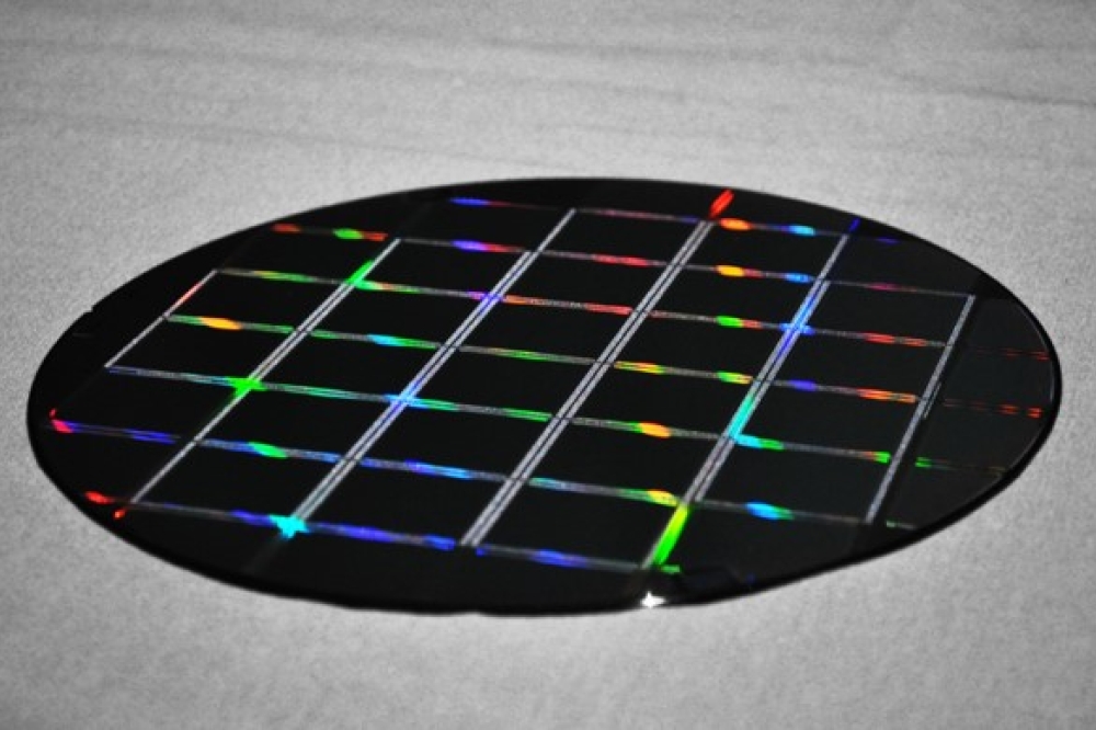
This type of electron-beam lithography system can "write" structures with a precision in the 10-nanometer range (approximately 1/2,000th of a hair) on substrates up to 300 mm in diameter.

The Vistec SB3050-2 electron-beam lithography system is based on the so-called Variable Shaped Beam principle, with which even large areas can be structured highly accurately and effectively. The high degree of automation, combined with flexibility in terms of usable substrates, are further features of the Vistec SB3050-2 that enable it to be used in an industrial environment. The system is equipped with Cell Projection functionality, opening up further possibilities for applications in micro-optics.

Jenoptik has been active in Dresden since 2007. With the new high-tech fab at Airportpark Dresden, the company is consolidating its production, which is currently spread across several small external sites, while at the same time expanding its capacities. The clean room production in the new fab will cover 2,000 square meters with clean room areas of classes ISO 5 and 3 and meet the highest requirements for freedom from vibrations and temperature stability.

High environmental standards are taken into account for the entire fab: Jenoptik is striving to fulfill the currently most comprehensive and stringent building criteria in terms of sustainability with the "KfW 40 Standard" and the "LEED Gold Standard Certification". At the same time, high-quality jobs will be created and the number of employees on site will increase to a total of more than 120. The Saxon state capital will thus become the main location for the micro-optics sector.

Silicon photonics: accelerating growth in the race for high-speed optical interconnects
CCD-in-CMOS technology enables ultra-fast burst mode imaging
2025 6G A look forward
Critical Manufacturing climbs Deloitte’s Technology Fast 50
Semiconductors: The most important thing you probably know the least about
Imec and partners unveil SWIR sensor with lead-free quantum dot photodiodes
Lattice introduces small and mid-range FPGA offerings
SEMI and SMT inspection solutions at NEPCON Japan 2025
Nordic Semiconductor and Kigen demonstrate Remote SIM Provisioning for Massive IoT
Spirent collaborates with Siemens
Quobly forges strategic collaboration with STMicroelectronics
New standards in pressure measurement systems for the semiconductor industry
IBM delivers optics breakthrough
Semiconductor equipment sales to reach $139 Billion in 2026
Marvell introduces 1.6 Tbps LPO Chipset
ACM research strengthens Atomic Layer Deposition portfolio
CEA-Leti demonstrates embedded FeRAM platform compatible with 22nm FD-SOI node
Lattice introduces small and mid-range FPGA offerings
Solace unlocks full potential of event-driven integration
Advantest to showcase latest test solutions at SEMICON Japan 2024
CEA-Leti device integrates light sensing and modulation
Nordic launches Thingy:91 X prototyping platform for cellular IoT and Wi-Fi locationing
Imec achieves seamless InP Chiplet integration on 300mm RF Silicon Interposer
High-precision SMU
Powering India’s energy future
China’s Nvidia probe puts global investors ‘on notice’
POET Technologies appoints new director
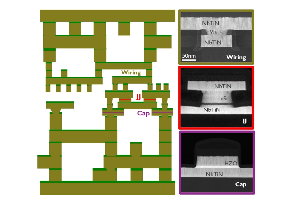
Imec demonstrates core building blocks of a scalable, CMOS-fab compatible superconducting digital technology
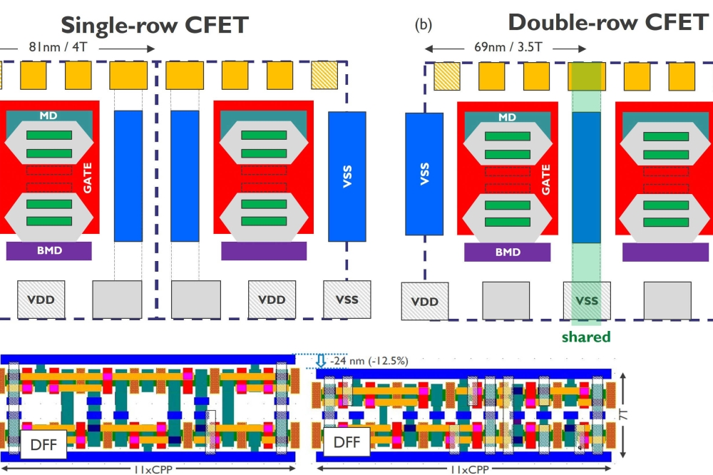
Imec proposes double-row CFET for the A7 technology node
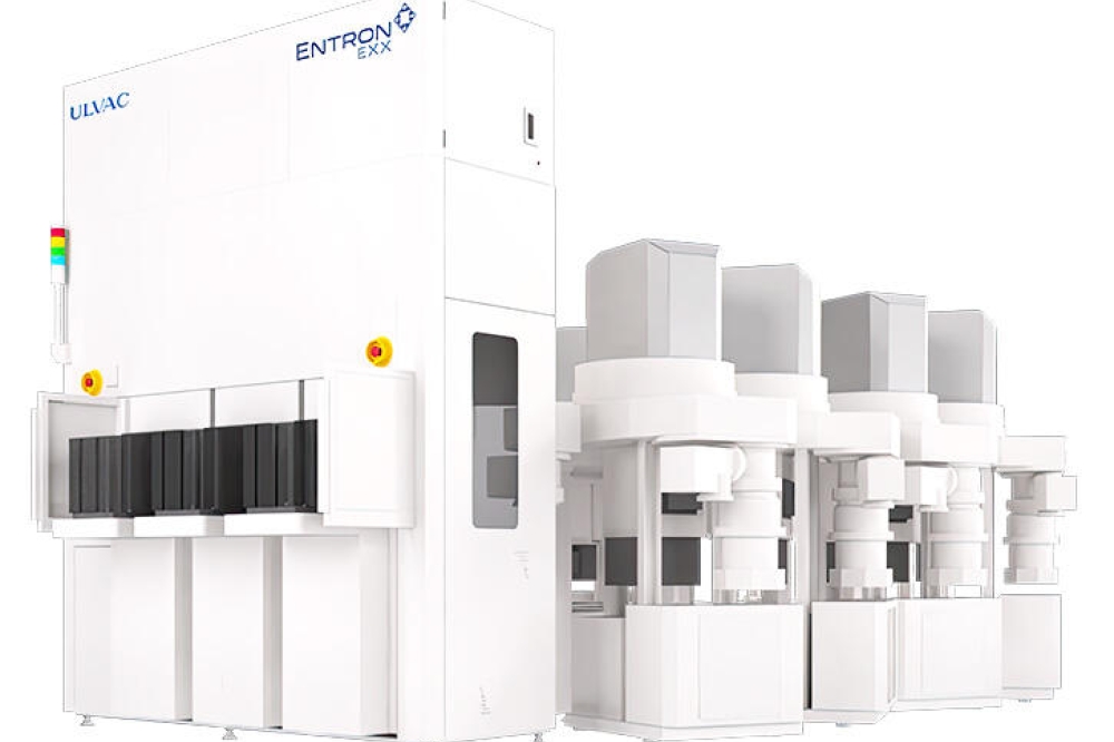
ULVAC launches new deposition system
Beebolt and SEMI Announce Strategic Partnership to Drive Supplier Resilience and Agility
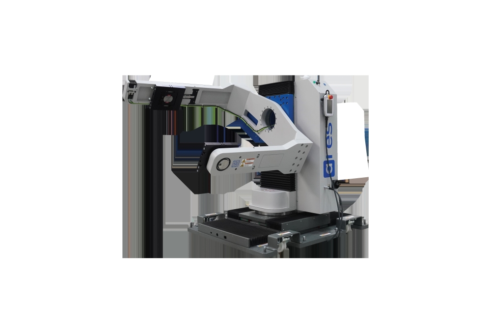
esmo group introduces Automated Final Test Manipulator
×
Search the news archive

To close this popup you can press escape or click the close icon.
Logo
x
Logo
×
Register - Step 1

You may choose to subscribe to the Silicon Semiconductor Magazine, the Silicon Semiconductor Newsletter, or both. You may also request additional information if required, before submitting your application.


Please subscribe me to:


You chose the industry type of "Other"

Please enter the industry that you work in: