News Article
Cadence acquires Invecas

Transaction brings Cadence skilled system design expertise in delivering end-to-end custom solutions to customers across multiple industries.
Cadence Design Systems has acquired Invecas, Inc., a leading provider of design engineering, embedded software and system-level solutions, headquartered in Santa Clara, California. The purchase adds a skilled system design engineering team to Cadence, with expertise in providing customers with custom solutions across chip design, product engineering, advanced packaging and embedded software.
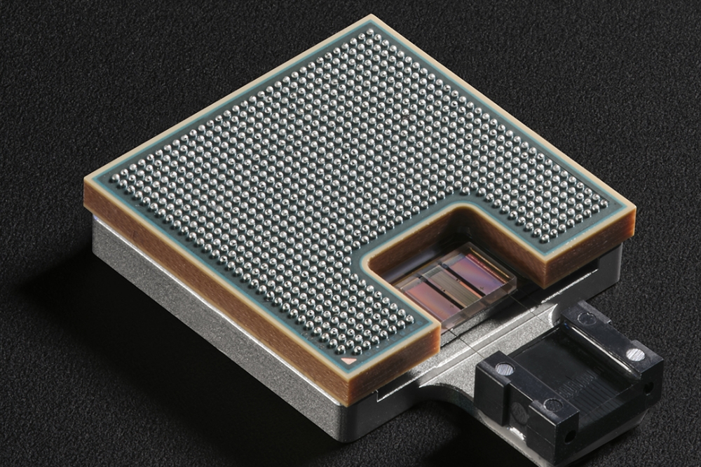
Accelerating trends such as digital transformation of multiple vertical markets and more system companies building custom silicon continue to drive strong design activity. Additionally, with classic Moore’s law slowing down, new “More than Moore” technologies, such as advanced 2.5D/3D packaging and chiplets, are paving the way for significant performance and manufacturing efficiencies. These strategic generational trends, underpinned by advancements in AI, are ushering in a new era of design and spurring a rapidly growing customer need for skilled end-to-end engineering expertise in enabling their custom silicon and system development efforts.
The acquisition brings a skilled engineering team centered in Hyderabad, led by Invecas CEO Dasaradha Gude, that has vast experience in delivering end-to-end system solutions with deep expertise in advanced nodes, mixed-signal, verification, embedded software, packaging and turnkey custom silicon production. Invecas has built close relationships with key players in the design ecosystem as well as with top foundry and assembly and test partners. With extensive experience designing chips and taking them to production, Invecas has served hundreds of customers across various verticals, including mobile, networking, hyperscaler and automotive. In addition to Cadence’s leading EDA solutions, Invecas will also leverage and augment Cadence’s broad IP portfolio to enable more comprehensive custom product solutions.
“With complexity and challenges increasing due to the proliferation of AI, 2.5D/3D and chiplet designs, customers need access to experienced teams that can assist with bringing designs from ideation to production,” said Boyd Phelps, senior vice president and general manager, Silicon Solutions Group, Cadence. “With the acquisition of Invecas, Cadence is able to scale our system design engineering offerings to support customers in critical high-growth verticals who are faced with the need to aggressively increase performance while tackling ever-increasing system-level complexity.”
“Generational trends are accelerating the increases in design complexity and driving a customer need for skilled engineering talent that can assist with system design,” said Dasaradha Gude, CEO, Invecas. “We are excited to join the Cadence team and to enhance the solutions available to customers, utilizing our core expertise to accelerate customer silicon and system development efforts.”
The terms of the transaction were not disclosed. The acquisition is expected to be immaterial to Cadence’s total revenue and earnings this year.


